background image

1-11-1

E5700TEST

FIRMWARE RENEWAL MODE

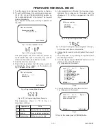
1. Turn the power on and remove the disc on the tray.
2. To put the DVD player into version up mode, press

[9], [8], [7], [6], and [SEARCH MODE] buttons on
the remote control unit in that order. The tray will
open automatically.
Fig. a appears on the screen and Fig. b appears on
the VFD.

The DVD player can also enter the version up
mode with the tray open. In this case, Fig. a will be
shown on the screen while the tray is open.

3. Load the disc for version up.
4. The DVD player enters the F/W version up mode

automatically. Fig. c appears on the screen and
Fig. d appears on the VFD.

The appearance shown in (*2) of Fig. c is
described as follows:

5. After programming is finished, the tray opens auto-

matically. Fig. e appears on the screen and the
checksum in (*3) of Fig. e appears on the VFD.
(Fig. f)

At this time, no buttons are available.

6. Unplug the AC cord from the AC outlet. Then plug it

again.

7. Turn the power on by pressing the power button

and the tray will close.

8. Press [1], [2], [3], [4], and [DISPLAY] buttons on the

remote control unit in that order. 
Fig. g appears on the screen.

9. Press [3] button on the remote control unit. 

Fig. h appears on the screen.

10.To exit this mode, press [POWER] button.

F/W Version Up Mode

   Please insert a DISC

for F/W Version Up.

EXIT: POWER

Fig. a  Version Up Mode Screen

Fig. b  VFD in Version Up Mode

Fig. c  Programming Mode Screen

F/W Version Up Mode

   VERSION :     ********
   Reading...(*2)

EXIT: POWER

Fig. d  VFD in Programming Mode (Example)

Appearance

No.

State

Reading...

Sending files into the memory

Erasing...

Erasing previous version data

Programming...

1

2

3

Writing new version data

Fig. e  Completed Program Mode Screen

F/W Version Up Mode

VERSION :     ********
Completed
SUM : 7abc (*3)

Fig. f  VFD upon Finishing the Programming Mode (Example)

Fig. g

model: ******

Ver: ****

Region: **

1: VFD TEST
2: TT REPEAT PLAY
3: EEPROM CLEAR
4: MEASUREMENT SERVO
5: DISC READ CHECK
6: MECHA CHECK
7: DISC INFO
8: ERROR RATE

EXIT: POWER

RETURN: -----

Fig. h

model: ******

Ver: ****

Region: **

TEST 3: EEPROM CLEAR
EEPROM CLEAR: OK

EXIT: POWER

RETURN: -----

Содержание DV4400

Страница 1: ...BLOCK DIAGRAMS 1 7 1 SCHEMATIC DIAGRAMS CBA S AND TEST POINTS 1 8 1 WAVEFORMS 1 9 1 WIRING DIAGRAMS 1 10 1 FIRMWARE RENEWAL MODE 1 11 1 LEAD IDENTIFICATIONS 1 12 1 EXPLODED VIEWS 1 13 1 PARTS LIST DV4400 1 14 1 PARTS LIST DV6400 1 15 1 DV6400 N1B N1S DV4400 DV6400 Please use this service manual with referring to the user guide D F U without fail Service Manual Part no 44AW855010 First Issue 2003 1...

Страница 2: ... JAPAN Technical MARANTZ JAPAN INC 35 1 7 CHOME SAGAMIONO SAGAMIHARA SHI KANAGAWA JAPAN 228 8505 PHONE 81 42 748 1013 FAX 81 42 741 9190 EUROPE TRADING MARANTZ EUROPE B V P O BOX 8744 BUILDING SILVERPOINT BEEMDSTRAAT 11 5653 MA EINDHOVEN THE NETHERLANDS PHONE 31 40 2507844 FAX 31 40 2507860 AUSTRALIA QualiFi Pty Ltd 24 LIONEL ROAD MT WAVERLEY VIC 3149 AUSTRALIA PHONE 61 0 3 9543 1522 FAX 61 0 3 95...

Страница 3: ...tal harmonic distortion 1kHz CD 0 003 4 Dynamic range DVD 100dB CD 98dB DIGITAL AUDIO OUTPUT Optical digital output Optical connector 1 set Coaxial digital output Pin jack 1 set POWER SUPPLY AC 230V 50Hz POWER CONSUMPTION 15W Standby 1 0W MAXIMUM EXTERNAL DIMENSIONS 440 width x 75 height x 211 depth mm MASS 2 1Kg 4 6 lbs REMOTE CONTROL UNIT RC6400DV Infrared pulse type Supply DC 3V 2 R6P AA batter...

Страница 4: ...nd then into subsections called tracks each of which is given an album or track number Example Title 1 Title 2 Chapter 1 Chapter 2 Chapter 1 Chapter 2 Chapter 3 Chapter 4 Example Track 1 Track 2 Track 3 Track 4 Track 5 Track 6 Example Group 1 Group 2 Track 1 Track 2 Track 1 Track 2 Track 3 Track 4 DVD Video NOTE 1 DVD R DVD RW NOTE 2 CD CD R CD RW NOTE 3 Picture CD Digital video MPEG2 Digital audi...

Страница 5: ...ing 2 CDs 4Hz to 20kHz 3 Super Audio CD 4Hz to 100kHz 2 S N ratio 115dB 3 Total harmonic distortion 1kHz CD 0 003 4 Dynamic range DVD 100dB CD 98dB DIGITAL AUDIO OUTPUT Optical digital output Optical connector 1 set Coaxial digital output Pin jack 1 set POWER SUPPLY AC 230V 50Hz POWER CONSUMPTION 16W Standby 1 2W MAXIMUM EXTERNAL DIMENSIONS 440 width x 75 height x 211 depth mm MASS 2 2Kg 4 9lbs RE...

Страница 6: ...ter 4 Example Track 1 Track 2 Track 3 Track 4 Track 5 Track 6 Example Group 1 Group 2 Track 1 Track 2 Track 1 Track 2 Track 3 Track 4 DVD Video NOTE 1 DVD Audio DVD R DVD RW NOTE 2 CD CD R CD RW NOTE 3 Picture CD Digital video MPEG2 Digital audio Digital audio MP3 WMA NOTE 4 Digital picture JPEG JPEG Mark logo Usable discs Recorded signals Disc Size 12 cm 12 cm 12 cm 12 cm 8 cm 8 cm NOTE 1 Some DV...

Страница 7: ...errors SBC444 Disc with DO errors black spots and fingerprints SBC444A 4822 397 30245 Disc 65 min 1kHz without no pause 4822 397 30155 Max diameter disc 58 0 mm 4822 397 60141 Torx screwdrivers Set straight 4822 395 50145 Set square 4822 395 50132 13th order filter 4822 395 30204 DVD test disc PAL 4822 397 10131 SERVICE HINTS ...

Страница 8: ...ols also at this potential WARNING Safety regulations require that the set be restored to its original condition and that parts which are identical with those specified be used Veiligheidsbepalingen vereisen dat het apparaat in zijn oorspronkelijke toestand wordt terug gebracht en dat onderdelen identiek aan de gespecifieerde worden toegepast Bei jeder Reparatur sind die geltenden Sicherheitsvorsc...

Страница 9: ...eyes at least 30cm away from the pickup lens when the diode is turned on Do not look directly at the laser beam Caution Use of controls and adjustments or doing procedures other than those specified herein may result in hazardous radiation exposure Do not look directly at the laser beam coming from the pickup or allow it to strike against your skin Drive Mecha Assembly Laser Beam Radiation Laser P...

Страница 10: ...especially 1 Wires covered with PVC tubing 2 Double insulated wires 3 High voltage leads D Use specified insulating materials for hazardous live parts Note especially 1 Insulation tape 2 PVC tubing 3 Spacers 4 Insulators for transistors E When replacing AC primary side components transformers power cord etc wrap ends of wires securely about the terminals before solder ing F Observe that the wires ...

Страница 11: ... 2 Leakage Current Test Confirm the specified or lower leakage current between B earth ground power cord plug prongs and externally exposed accessible parts RF termi nals antenna terminals video and audio input and output terminals microphone jacks earphone jacks etc is lower than or equal to the specified value in the table below Measuring Method Power ON Insert load Z between B earth ground powe...

Страница 12: ...ve the flat pack IC with tweezers while apply ing the hot air 3 Bottom of the flat pack IC is fixed with glue to the CBA when removing entire flat pack IC first apply soldering iron to center of the flat pack IC and heat up Then remove glue will be melted Fig S 1 6 4 Release the flat pack IC from the CBA using twee zers Fig S 1 6 Caution 1 Do not supply hot air to the chip parts around the flat pa...

Страница 13: ...l pins of the flat pack IC you can remove it easily Fig S 1 3 2 Affix the wire to a workbench or solid mounting point as shown in Fig S 1 5 3 While heating the pins using a fine tip soldering iron or hot air blower pull up the wire as the solder melts so as to lift the IC leads from the CBA contact pads as shown in Fig S 1 5 4 Bottom of the flat pack IC is fixed with glue to the CBA when removing ...

Страница 14: ...ur due to a potential difference caused by electro static charge during unpacking or repair work 1 Ground for Human Body Be sure to wear a grounding band 1MΩ that is prop erly grounded to remove any static electricity that may be charged on the body 2 Ground for Workbench 1 Be sure to place a conductive sheet or copper plate with proper grounding 1MΩ on the workbench or other surface where the sem...

Страница 15: ...02 1 7 Release two Locking Tabs L 2 Then release five Locking Tabs L 3 to do this first release two Locking Tabs A at the side and then three Locking Tabs B at the bottom CAUTION 2 Electrostatic breakdown of the laser diode in the optical system block may occur as a potential difference caused by electrostatic charge accumulated on cloth human body etc during unpacking or repair work To avoid dama...

Страница 16: ...of pickup will be destroyed Fig D6 CAUTION 3 When reassembling confirm the FFC cable CN201 is connected completely Then remove the solder from the three short lands of FPC cable Fig D6 S 1 S 1 S 1 1 Top Cover Fig D1 2 Front Unit Tray Panel A A L 3 L 2 CN2002 L 1 L 1 B Fig D2 3 Function CBA S 2 S 2 Insulation Sheet 4 Front Assembly Fig D3 S 4 S 4 S 4 S 3 5 Rear Panel Fig D4 ...

Страница 17: ...01 CN1001 6 DVD Mecha 7 DVD Main CBA Unit 8 DVD Main CBA Holder Fig D5 A DVD Mecha View for B Pickup Unit C Short the three short lands by soldering Short the three short lands by soldering FPC Cable Connector Slide View for C View for A OR Fig D6 ...

Страница 18: ...N6001 L 4 L 5 L 5 10 Switch CBA Desolder 11 LED CBA 12 LED CBA Holder Fig D7 HOW TO MANUAL EJECT 1 Remove the Top Case 2 Rotate the roulette in the direction of the arrow as shown below Rotate this roulette in the direction of the arrow A View for A ...

Страница 19: ...se two Locking Tabs L 7 Then release five Locking Tabs L 8 to do this first release two Locking Tabs A at the side and then three Locking Tabs B at the bottom CAUTION 2 Electrostatic breakdown of the laser diode in the optical system block may occur as a potential difference caused by electrostatic charge accumulated on cloth human body etc during unpacking or repair work ID LOC No PART REMOVAL Fi...

Страница 20: ...m it If you disconnect the FFC cable CN201 the laser diode of pickup will be destroyed Fig D13 CAUTION 3 When reassembling confirm the FFC cable CN201 is connected completely Then remove the solder from the three short lands of FPC cable Fig D13 S 11 S 11 S 11 1 Top Cover Fig D8 2 Front Unit Tray Panel A A L 8 L 7 CN2002 L 6 L 6 B Fig D9 3 Function CBA S 12 S 12 Insulation Sheet 4 Front Assembly F...

Страница 21: ...601 CN1001 CN7101 6 DVD Mecha 9 DVD Main CBA Unit 10 DVD Main CBA Holder 7 Shield Plate 8 SACD CBA Fig D12 A DVD Mecha View for B Pickup Unit C Short the three short lands by soldering Short the three short lands by soldering FPC Cable Connector Slide View for C View for A OR Fig D13 ...

Страница 22: ...CN6001 L 10 L 11 L 11 12 Switch CBA Desolder 13 LED CBA 14 LED CBA Holder Fig D14 Rotate this roulette in the direction of the arrow A View for A HOW TO MANUAL EJECT 1 Remove the Top Case 2 Rotate the roulette in the direction of the arrow as shown below ...

Страница 23: ...riphery circuit and service it if defective Check if there is any leak or short circuit on the loaded circuit and service it if defective Yes No FLOW CHART NO 1 The power cannot be turned on Is the fuse normal Is normal state restored when once unplugged power cord is plugged again after several seconds Is the EV 9V line voltage normal Is each voltage of the secondary side normal See FLOW CHART No...

Страница 24: ...er on Replace Q1002 Check D1030 D1048 D1053 C1035 C1048 L1009 and the periphery circuit and service it if defective Check Q1016 and PWRCON line and service it if defective Yes Yes No No FLOW CHART NO 10 EV 1 5V is not outputted Is 2 5V voltage supplied to Pin 1 of IC1002 Is 1 25V voltage supplied to Pin 4 of IC1002 Replace IC1002 Replace IC2002 Check the circuit between Pin 19 of IC2002 and Pin 4 ...

Страница 25: ... Yes Yes No No No No FLOW CHART NO 12 The fluorescent display tube does not light up Is 5V voltage supplied to Pin 13 and Pin 43 of IC6001 Is the voltage of approximately 24V to 28V supplied to Pin 30 of IC6001 Is there 500kHz oscillation at Pin 5 of IC6001 Are the filament voltage supplied between Pins 1 2 and Pins 34 35 of the fluorescent display tube And the negative voltage applied between the...

Страница 26: ...LOSE button SW6406 No FLOW CHART NO 14 No operation is possible from the remote control unit Operation is possible from the DVD but no operation is possible from the remote control unit Replace the infrared remote control receiver RM2001 Or replace the remote control unit Check the line between Pin 20 of IC2002 and Pin 22 of CN1001 and service it if detective Is the L pulse sent out Pin 1 terminal...

Страница 27: ...Main CBA is poor FLOW CHART NO 18 No Disc indicated When the focus servo is not functioning FLOW CHART NO 19 No Disc indicated When the laser beam does not light up Replace the DVD Main CBA Replace the DVD Mecha No Yes Replace the DVD Main CBA Replace the DVD Mecha No Yes No improvement can be found Original DVD Main CBA is poor No improvement can be found Original DVD Main CBA is poor ...

Страница 28: ...S C IC6101 16PIN G IC6101 12PIN B Cb IC6101 14PIN R Cr IC6101 31PIN CVBS IC6101 28PIN S Y IC6101 33PIN S C IC6101 19PIN G IC6101 25PIN B Cb IC6101 22PIN R Cr Check the periphery of JK6101 from Pins 19 22 25 of IC6101 and service it if defective Check the periphery of JK6102 from Pin 22 25 28 of IC6101 and service it if defective Check the periphery of JK1401 from Pin 28 of IC6101 and service it if...

Страница 29: ...IO R Replace the DVD Main CBA or DVD Mecha Replace the DVD Main CBA or DVD Mecha Replace IC1201 Check the periphery between Pins 1 7 of IC1201 and JK6103 and service it if detective Check each line between each pin of CN1601 and each pin of IC1201 on AV CBA and service it if detective CN1601 13PIN IC1201 6PIN AUDIO L CN1601 15PIN IC1201 2PIN AUDIO R Are the analog audio signals inputted to each pi...

Страница 30: ... each pin of IC7301 IC7401 and IC7501 IC7301 1 7PIN FRONT L R IC7401 1 7PIN SORROUND L R IC7501 1 7PIN CENTER SUBWOOFER SORROUND L CN7102 19PIN IC7202 14PIN SORROUND R CN7102 19PIN IC7202 13PIN CENTER CN7102 19PIN IC7203 14PIN SUBWOOFER CN7102 19PIN IC7203 13PIN Do the mute signals of each line as shown below become to H level FRONT L CN7102 18PIN IC7201 14PIN FRONT R CN7102 18PIN IC7201 13PIN Is ...

Страница 31: ...ve continued to A on next page Audio is not outputted to JK7101 normally 2 FLOW CHART NO 24 FOR DV6400 N1B DV6400 N1S IC7201 1PIN DSD L IC7201 2PIN DSD R IC7202 1PIN DSD LS IC7202 2PIN DSD RS IC7203 1PIN DSD C IC7203 2PIN DSD SW Replace the DVD Main CBA Unit or DVD Mecha CN7102 7PIN IC7251 170PIN PCM DATA0 CN7102 5PIN IC7251 171PIN PCM DATA1 CN7102 3PIN IC7251 172PIN PCM DATA2 CN7102 1PIN IC7251 1...

Страница 32: ...NT L CN7102 18PIN IC7201 14PIN FRONT R CN7102 18PIN IC7201 13PIN Is the analog audio signal of each line outputted to each terminal of JK7101 as shown below IC7301 1PIN JK7101 FRONT L IC7301 7PIN JK7101 FRONT R IC7401 1PIN JK7101 SORROUND L IC7401 7PIN JK7101 SORROUND R IC7501 1PIN JK7101 CENTER IC7501 7PIN JK7101 SUBWOOFER Yes Yes No No No No No Replace the DVD Main CBA Unit or IC7203 Check each ...

Страница 33: ...RVO SIGNAL SLED SERVO SIGNAL SPINDLE SERVO SIGNAL 3 SP 4 SP 5 TRAY OUT 6 TRAY IN 7 GND 8 SL 9 SL 1 FG IN 64 ASPECT ASPECT FP STB FP DIN FP DOUT REMOTE FP CLK REMOTE SENSOR RM2001 K1 REMOTE OUT FIP SEGMENT FL2001 IC6001 FRONT PANEL CONTROL IC2002 ENERGY STAR MICROCONTROLLER 20 REMOTE IN 13 PWRCON PWRCON PWSW AD KEY PWSW 18 8 19 KEY MATRIX CN2002 Q2007 CN6401 16 FP STB 16 18 FP DIN 18 20 FP DOUT 20 ...

Страница 34: ...ST ROM SERIAL D A GENERAL I O INTERRUPT CONTROLLER TIMER WATCH DOG TIMER 32BIT CPU STREAM I F EXTERNAL MEMORY I F SDRAM ECC UMAC 124 125 122 123 128 129 126 127 131 130 135 133 132 134 78 DEBUG BCU INST CACHE D TYPE LATCH DATA CACHE D A D A D A TO VIDEO AUDIO BLOCK DIAGRAM 158 164 G C R Cr B Cb VIDEO G VIDEO C VIDEO R Cr VIDEO B Cb TO VIDEO AUDIO BLOCK DIAGRAM 181 SPDIF 175 PCM BCK 176 PCM DATA0 1...

Страница 35: ...SCLK AV CBA DVD MAIN CBA UNIT AUDIO SIGNAL DATA AUDIO SIGNAL 18 18 SPDIF A MUTE 3 3V JK6102 Q1204 WF6 5 WF4 WF5 CN601 VIDEO Y VIDEO C FROM DIGITAL SIGNAL PROCESS BLOCK DIAGRAM VIDEO SIGNAL 5V JK6101 1 3 AUDIO L OUT AUDIO R OUT FIBER OPTIC TRANS MODULE IC1204 JK1401 S VIDEO OUT COMPOSITE VIDEO OUT CN1601 1 1 VIDEO Y 9 9 VIDEO C 3 4 2 1 IC6101 VIDEO DRIVER 6 28 4dB AMP 2dB AMP LPF DRIVER Y C 2 33 4d...

Страница 36: ... CN1001 Q1004 FL EV 5V F2 F1 P ON 12V EV 3 3V P ON 5V P ON 3 3V FROM TO CN401 1 2 3 EV 1 5V 4 5 EV 3 3V 14 15 EV 9V 13 P ON 5V 17 P ON 3 3V 1 5V REG IC1002 CAUTION Fixed voltage or Auto voltage selectable power supply circuit is used in this unit If Main Fuse F1001 is blown check to see that all components in the power supply circuit are not defective before you connect the AC plug to the AC power...

Страница 37: ...DAC ML2 20 88 89 84 REMOTE SENSOR RM2001 K1 REMOTE OUT FIP SEGMENT FL2001 IC6001 FRONT PANEL CONTROL IC2002 ENERGY STAR MICROCONTROLLER 20 REMOTE IN 13 PWRCON PWRCON PWSW AD KEY PWSW 18 8 19 KEY SWITCH CN2002 Q2007 CN6401 16 FP STB 16 18 FP DIN 18 20 FP DOUT 20 21 FP CLK 21 22 REMOTE 22 19 PWRCON 19 2 KEY 2 2 5 K2 5 8 K1 8 3 KEY 1 3 4 KEY 3 4 7 KEY 8 7 9 KEY 7 9 11 KEY 6 11 6 KEY 4 6 1 AD KEY 1 59...

Страница 38: ...CM BCK PCM BCK 176 PCM DATA3 PCM DATA3 PCM DATA2 PCM DATA1 PCM DATA0 174 178 179 180 PCM LRCLK PCM LRCLK 161 160 EXADT 0 15 EXADR 16 19 EXADT 0 15 EXADR 16 19 EXADT 0 7 EXADT 8 15 EXADR 0 7 EXADR 0 15 EXADR 8 15 SDRAM DATA 0 31 SDRAM DATA 0 31 SDRAM ADDRESS 0 10 SDRAM ADDRESS 0 10 2 9 12 19 210 235 IC104 LATCH D TYPE LATCH 2 9 12 19 2 13 184 205 247 256 2 13 31 56 74 85 IC103 FLASH ROM FLASH ROM 2...

Страница 39: ... S VIDEO OUT 3 4 2 1 Y C COMPOSITE VIDEO OUT VIDEO Cb OUT VIDEO Y OUT VIDEO Cr OUT JK6103 VIDEO SIGNAL 5V WF3 FIBER OPTIC TRANS MODULE IC1204 JK6102 Q1601 Q1602 AMP AND GATE IC902 2 1 Video Audio Block Diagram DV6400 N1B DV6400 N1S TO SYSTEM CONTROL SERVO BLOCK DIAGRAM TO DIGITAL SIGNAL PROCESS BLOCK DIAGRAM DVD MAIN CBA UNIT AV CBA CN601 9 9 VIDEO C 3 3 VIDEO R Cr 7 7 VIDEO G 5 5 VIDEO B Cb VIDEO...

Страница 40: ... FILTER LPF LPF MODE CONTROL PCM SYSTEM CLOCK IC7203 AUDIO D A CONVERTER MULTI LEVEL DELTA SIGMA MODULATOR DSD I F 20 9 10 14 13 1 2 3 4 5 15 16 17 18 PCM I F DSD FILTER MUX DAC PCM FILTER LPF LPF MODE CONTROL PCM SYSTEM CLOCK 6 2 7 1 FRONT R OUT FRONT L OUT JK7101 SURROUND R OUT SURROUND L OUT CENTER OUT SUB WOOFER OUT 15 IECOUT 16 PHCOPMO 1 PCM DATA3 3 PCM DATA2 5 PCM DATA1 7 PCM DATA0 9 PCM BCK...

Страница 41: ... PWSW 3 P ON 9V 6 P ON 3 3V 7 P ON 3 3V 1 P ON 5V EV 3 3V CN1603 NOTE The voltage for parts in hot circuit is measured using hot GND as a common terminal Power Supply Block Diagram DV6400 N1B DV6400 N1S CAUTION Fixed voltage or Auto voltage selectable power supply circuit is used in this unit If Main Fuse F1001 is blown check to see that all components in the power supply circuit are not defective...

Страница 42: ...titute replacement parts that do not have the same safety characteristics as speci fied in the parts list may create shock fire or other hazards Notes 1 Do not use the part number shown on these draw ings for ordering The correct part number is shown in the parts list and may be slightly different or amended since these drawings were prepared 2 All resistance values are indicated in ohms K 103 M 1...

Страница 43: ...red units use only original replacement parts which are listed with their part numbers in the parts list section of the service manual 4 Wire Connectors 1 Prefix symbol CN means connector can disconnect and reconnect 2 Prefix symbol CL means wire solder holes of the PCB wire is soldered directly 5 Voltage indications for PLAY modes on the schematics are as shown below 6 How to read converged lines...

Страница 44: ...DVD Main 1 3 Schematic Diagram DV4400 N1B DV4400 N1S 1 8 3 1 8 4 E57M2SCD1 ...

Страница 45: ...DVD Main 2 3 Schematic Diagram DV4400 N1B DV4400 N1S 1 8 5 1 8 6 E57M2SCD2 ...

Страница 46: ... 127 2 0 2 0 32 64 0 8 0 8 96 3 4 3 4 128 2 0 2 0 PIN NO PLAY STOP PIN NO PLAY STOP PIN NO PLAY STOP PIN NO PLAY STOP 129 2 0 2 0 161 0 5 0 5 193 225 1 9 1 9 130 2 2 2 2 162 1 4 1 4 194 0 0 226 3 3 3 3 131 2 3 2 3 163 1 4 1 4 195 3 3 3 3 227 132 0 4 0 1 164 0 9 0 9 196 228 133 1 2 0 4 165 3 3 3 3 197 229 134 0 4 0 1 166 1 5 1 5 198 0 0 230 0 0 135 0 2 0 2 167 0 0 199 231 136 2 3 2 3 168 2 1 2 1 20...

Страница 47: ...DVD Main 3 3 Schematic Diagram DV4400 N1B DV4400 N1S 1 8 9 1 8 10 E57M2SCD3 ...

Страница 48: ...wn check to see that all components in the power supply circuit are not defective before you connect the AC plug to the AC power supply Otherwise it may cause some components in the power supply circuit to fail NOTE THE VOLTAGE FOR PARTS IN HOT CIRCUIT IS MEASURED USING HOT GND AS A COMMON TERMINAL CAUTION FOR CONTINUED PROTECTION AGAINST FIRE HAZARD REPLACE ONLY WITH THE SAME TYPE FUSE ...

Страница 49: ...AV 2 3 Schematic Diagram DV4400 N1B DV4400 N1S 1 8 13 1 8 14 E57M2SCAV2 ...

Страница 50: ... g h i a b a b a b a b a b FL2001 MATRIX CHART STANDBY TITLE CHP TRK CD V PBC DVD REPEAT A B 1 3 2 4 5 1 8 15 1 8 16 7G 5G 3G 1G 4G 6G 2G a d g c b e f 1 3 2 4 5 DVD VCD PBC STANDBY A B REPEAT TRK CHP TITLE E57M2SCAV3 AV 3 3 Function Switch LED Schematic Diagram DV4400 N1B DV4400 N1S ...

Страница 51: ...DVD Main 1 3 Schematic Diagram DV6400 N1B DV6400 N1S 1 8 17 1 8 18 E57M7SCD1 ...

Страница 52: ...DVD Main 2 3 Schematic Diagram DV6400 N1B DV6400 N1S 1 8 19 1 8 20 E57M7SCD2 ...

Страница 53: ...62 3 3 3 3 94 3 6 3 6 126 2 0 2 0 31 63 3 4 3 4 95 3 4 0 1 127 2 0 2 0 32 64 0 8 0 8 96 3 4 3 4 128 2 0 2 0 PIN NO PLAY STOP PIN NO PLAY STOP PIN NO PLAY STOP PIN NO PLAY STOP 129 2 0 2 0 161 0 5 0 5 193 225 1 9 1 9 130 2 2 2 2 162 1 4 1 4 194 0 0 226 3 3 3 3 131 2 3 2 3 163 1 4 1 4 195 3 3 3 3 227 132 0 4 0 1 164 0 9 0 9 196 228 133 1 2 0 4 165 3 3 3 3 197 229 134 0 4 0 1 166 1 5 1 5 198 0 0 230 ...

Страница 54: ...1 8 23 1 8 24 E57M7SCD3 DVD Main 3 3 Schematic Diagram DV6400 N1B DV6400 N1S ...

Страница 55: ...wn check to see that all components in the power supply circuit are not defective before you connect the AC plug to the AC power supply Otherwise it may cause some components in the power supply circuit to fail NOTE THE VOLTAGE FOR PARTS IN HOT CIRCUIT IS MEASURED USING HOT GND AS A COMMON TERMINAL CAUTION FOR CONTINUED PROTECTION AGAINST FIRE HAZARD REPLACE ONLY WITH THE SAME TYPE FUSE ...

Страница 56: ...1 8 27 1 8 28 E57M7SCAV2 AV 2 3 Schematic Diagram DV6400 N1B DV6400 N1S ...

Страница 57: ...V6400 N1S 7G 6G 5G 4G 3G 2G 1G a b c d e f g c d e f g c d e f g c d e f g c d e f g c d e f g h i a b a b a b a b a b FL2001 MATRIX CHART STANDBY TITLE CHP TRK CD V PBC DVD REPEAT A B 1 3 2 4 5 7G 5G 3G 1G 4G 6G 2G a d g c b e f 1 3 2 4 5 DVD VCD PBC STANDBY A B REPEAT TRK CHP TITLE ...

Страница 58: ...1 8 31 1 8 32 SACD 1 2 Schematic Diagram DV6400 N1B DV6400 N1S E57M7SCSA1 ...

Страница 59: ...1 8 33 1 8 34 SACD 2 2 Schematic Diagram DV6400 N1B DV6400 N1S E57M7SCSA2 ...

Страница 60: ...age or Auto voltage selectable power supply circuit is used in this unit If Main Fuse F1001 is blown check to see that all components in the power supply circuit are not defective before you connect the AC plug to the AC power supply Otherwise it may cause some components in the power supply circuit to fail CAUTION FOR CONTINUED PROTECTION AGAINST FIRE HAZARD REPLACE ONLY WITH THE SAME TYPE FUSE ...

Страница 61: ... measured using hot GND as a common terminal CAUTION Fixed voltage or Auto voltage selectable power supply circuit is used in this unit If Main Fuse F1001 is blown check to see that all components in the power supply circuit are not defective before you connect the AC plug to the AC power supply Otherwise it may cause some components in the power supply circuit to fail CAUTION FOR CONTINUED PROTEC...

Страница 62: ...ew 1 8 39 BE57E2F01016 C 1 8 40 LED CBA Top View DV4400 N1B DV4400 N1S DV6400 N1B DV6400 N1S LED CBA Bottom View DV4400 N1B DV4400 N1S DV6400 N1B DV6400 N1S BE57E2F01016 B Switch CBA Top Bottom View DV4400 N1B DV4400 N1S DV6400 N1B DV6400 N1S ...

Страница 63: ...Function CBA Top View DV4400 N1B DV4400 N1S DV6400 N1B DV6400 N1S Function CBA Bottom View DV4400 N1B DV4400 N1S DV6400 N1B DV6400 N1S 1 8 41 BE57M7F01011 1 8 42 ...

Страница 64: ...SACD CBA Top View DV6400 N1B DV6400 N1S 1 8 43 BE57D1F02011 1 8 44 ...

Страница 65: ...SACD CBA Bottom View DV6400 N1B DV6400 N1S BE57D1F02011 1 8 45 1 8 46 ...

Страница 66: ...TOP MODE WF1 WF3 WAVEFORMS WF6 SPDIF Pin 18 of CN1601 1V 0 1µsec WF1 Pin 1 of CN1601 WF3 Pin 31 of IC6101 WF4 AUDIO L Pin 13 of CN1601 1V 0 5msec WF5 AUDIO R Pin 15 of CN1601 1V 0 5msec WF2 Pin 9 of CN1601 VIDEO Y 0 2V 20µsec VIDEO C 0 2V 20µsec VIDEO CVBS 0 5V 20µsec ...

Страница 67: ... AUDIO R OUT VIDEO OUT VIDEO Y OUT VIDEO Cb OUT VIDEO Cr OUT DIGITAL AUDIO OUT S VIDEO OUT EV 1 5V 3 3 DRIVE CBA 19 20 SPDIF 18 18 AUDIO L 13 13 A L MUTE 14 14 AUDIO R 15 15 A R MUTE 16 16 AUDIO 5V 17 17 1 GND 1 T RESET 2 SDATA 3 EV 3 3V 4 EXTRG0 5 GND 6 SCLOCK VREF P ON 5V F E C B D A PD MONI DVD LD GND LD GND DVD PD TS FS FS TS GND CD PD CD LD CD DVD FS TS DETECTOR 11 2 3 5 6 4 7 FG CBA FG SENSO...

Страница 68: ...4 14 AUDIO R 15 15 A R MUTE 16 16 AUDIO 5V 17 17 W1601 ASPECT 2 2 VIDEO Y 1 1 1 10 3 1 10 4 CN201 CN301 1 2 3 4 TRAY OUT TRAY IN GND 5 6 SP 7 SP 8 SL 9 SL FG IN P ON 3 3V D 1 2 3 4 5 6 7 8 9 10 11 12 13 14 15 16 17 18 TRAY IN AC CORD AUDIO L OUT AUDIO R OUT VIDEO OUT DIGITAL AUDIO OUT S VIDEO OUT OPTICAL AUDIO OUT 19 20 VIDEO Y OUT VIDEO Cb OUT VIDEO Cr OUT GND VREF P ON 5V F E C B D A PD MONI DVD...

Страница 69: ...let Then plug it again 7 Turn the power on by pressing the power button and the tray will close 8 Press 1 2 3 4 and DISPLAY buttons on the remote control unit in that order Fig g appears on the screen 9 Press 3 button on the remote control unit Fig h appears on the screen 10 To exit this mode press POWER button F W Version Up Mode Please insert a DISC for F W Version Up EXIT POWER Fig a Version Up...

Страница 70: ...2SK3566 PQ070XF01SZ K A R 1 2 3 4 Note A Anode K Cathode E Emitter C Collector B Base R Reference G Gate D Drain S Source 1 Vin 2 Vo 3 GND 4 Vc 34 18 17 MM1567AJ 1 GP1FA513TZ 1 2 3 20 11 10 1 M34506M4 506FP DSD1702E 2K 33 PT6315 12 22 23 11 1 44 34 132 CXD2753R 45 88 89 44 1 176 133 50 26 25 K4S161622D TC80 1 2SC2412K T146S KRA105S RTK KTC3875GR RTK C B E 1 3 6 4 NC7SB3157P6X 1 3 5 4 NC7SZ08P5X 1 ...

Страница 71: ...02 JK1401 JK6103 JK6102 IC1204 2L031 2B20 2L031 2L052 2L052 2L052 Function CBA A1X 2B36 JK6101 2B19 W6001 2B2 2L051 Switch CBA LED CBA 2B3 2L101 2L105 DVD Main CBA Unit 2B32 2L051 A17 A15 A13 A14 A14 A13 2B10 A16 1B1 A2 2L011 2L011 2L011 2L021 2L021 2L023 2L023 2L031 2L031 2B23 AC1001 F1001 2B33 EXPLODED VIEWS Cabinet DV4400 N1B DV4400 N1S A17 A17 A15 A18 A17 ...

Страница 72: ...A 2L031 W6001 W2002 1B1 2L021 A2 2L021 JK1202 JK1401 A13 A14 A14 A A A13 JK6103 JK6102 IC1204 F1001 2L031 2L031 B 2B2 2L051 2L023 2B10 2L023 2L041 W1601 W1603 W1001 2L105 2B12 2L104 B 2B32 2L051 LED CBA A17 2B8 2B19 2B20 2L031 2B23 DVD Main CBA Unit A15 SACD CBA A19 2L105 2L105 2B3 A17 2L101 W7102 W7151 JK6101 2B8 2B8 2B36 2L052 2L052 2L052 Function CBA A18 A1X DV6400 N1B DV6400 N1S ...

Страница 73: ...1 13 3 E57M2EX X10 X2 X4 S2 S2 S4 Unit S1 X13 X1 X5 A22 Packing ...

Страница 74: ...Y Switch CBA ASSY 0VSA14682 A18 ZZ002250R ZZ002250R PCB ASSY FUNCTION CBA ASSY 0VSA14617 AC1001 N S YC000820R YC000820R MAINS CORD MAINS CORD PE8B2CG980A 057 WAE0172LW006 AC1001 F nsp YC000830R MAINS CORD MAINS CORD PP8B5PB110AA057 WAJ0172LW009 AC1001 U nsp YC000840R MAINS CORD MAINS CORD A0A0280 007 OR PB8K9F9110A 057 WAC0172LTE04 OR WAC0172LW008 W1001 YU001380R YU001380R FPC 22P FFC AV PCB TO MA...

Страница 75: ...RMINAL S TYPE JACK MDC 050V 2 4 JXEL040LY001 JK1405 F nsp YT003560R TERMINAL D TERMINAL 14P DT 0102 001 JBDTJ14JD002 JK6101 N YT003390R YT003390R TERMINAL SCART CONNECTOR 21P RGB AJ 2050 040 JXGL210JD002 JK6102 N S U YT003400R YT003400R TERMINAL CINCH JACK 3PIN MSD 243V 18 NI JXRL030LY073 JK6103 YT003410R YT003410R TERMINAL CINCH JACK 3PIN MSD 243V 15 NI JXRL030LY079 L1001 F U nsp FN000200R FILTER...

Страница 76: ...Y FUNCTION CBA ASSY 0VSA14617 A19 N S ZZ002280R ZZ002280R PCB ASSY SACD CBA ASSY 0VSA14446 A19 F U nsp ZZ002410R PCB ASSY SACD CBA ASSY 0VSA14758 AC1001 N S YC000820R YC000820R MAINS CORD MAINS CORD PE8B2CG980A 057 WAE0172LW006 AC1001 F nsp YC000830R MAINS CORD MAINS CORD PP8B5PB110AA057 WAJ0172LW009 AC1001 U nsp YC000840R MAINS CORD MAINS CORD A0A0280 007 OR PB8K9F9110A 057 WAC0172LTE04 OR WAC017...

Страница 77: ...AL CINCH JACK BLACK MSP 251V 10 GILT JXRL010LY090 JK1401 YT003380R YT003380R TERMINAL S TYPE JACK MDC 050V 2 4 JXEL040LY001 JK1405 F nsp YT003560R TERMINAL D TERMINAL 14P DT 0102 001 JBDTJ14JD002 JK6101 N YT003390R YT003390R TERMINAL CINCH JACK 21P RGB AJ 2050 040 JXGL210JD002 JK6102 N S U YT003430R YT003430R TERMINAL CINCH JACK 3PIN MSD 243V 19 GILT JXRL030LY092 JK6103 YT003440R YT003440R TERMINA...

Отзывы: