1-6-9
E57M2TR
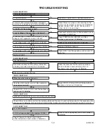
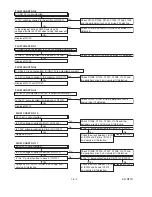
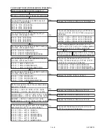
Set the disc (with Super Audio) on the disc tray, and playback.
Are the PCM data signals inputted to each pin
of CN7102 on SACD CBA?
Are the DSD data signals outputted to each pin
of IC7251?
CN7102 7PIN PCM-DATA0
CN7102 5PIN PCM-DATA1
CN7102 3PIN PCM-DATA2
CN7102 1PIN PCM-DATA3
Are the DSD data signals inputted to each pin
of IC7201, IC7202 and IC7203?
IC7251 170PIN PCM-DATA0
IC7251 171PIN PCM-DATA1
IC7251 172PIN PCM-DATA2
IC7251 173PIN PCM-DATA3
IC7251 64PIN DSD-L
IC7251 66PIN DSD-R
IC7251 74PIN DSD-LS
IC7251 76PIN DSD-RS
IC7251 69PIN DSD-C
IC7251 71PIN DSD-SW
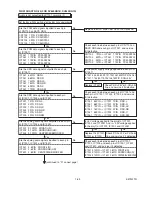
IC7251 64PIN
→
IC7201 1PIN DSD-L
IC7251 66PIN
→
IC7201 2PIN DSD-R
IC7251 74PIN
→
IC7202 1PIN DSD-LS
IC7251 76PIN
→
IC7202 2PIN DSD-RS
IC7251 69PIN
→
IC7203 1PIN DSD-C
IC7251 71PIN
→
IC7203 2PIN DSD-SW
Are the PCM data signals inputted to each pin
of IC7251?
Is the power supply voltage applied to each pin of
IC7251?
Check each line between each pin of CN7102 on
SACD CBA and each pin of IC7251, and service
it if defective.
Check each line between each pin of IC7251 and
each pin of IC7201, IC7202, IC7203, and service
it if defective.
Replace IC7251.
Check P-ON+2.5V or P-ON+3.3V
line, and service it if defective.
(continued to "A" on next page)
Audio is not outputted to JK7101 normally. (2)
FLOW CHART NO.24 (FOR DV6400/N1B, DV6400/N1S)
IC7201 1PIN DSD-L
IC7201 2PIN DSD-R
IC7202 1PIN DSD-LS
IC7202 2PIN DSD-RS
IC7203 1PIN DSD-C
IC7203 2PIN DSD-SW
Replace the DVD Main CBA Unit or DVD Mecha.
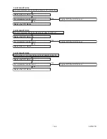
CN7102 7PIN
→
IC7251 170PIN PCM-DATA0
CN7102 5PIN
→
IC7251 171PIN PCM-DATA1
CN7102 3PIN
→
IC7251 172PIN PCM-DATA2
CN7102 1PIN
→
IC7251 173PIN PCM-DATA2
IC7251 5,35,54,83,99,121,124,125,153PIN: P-ON+2.5V
IC7251 17,45,90,110,135,146,163PIN: P-ON+3.3V
Yes
Yes
Yes
Yes
No
No
No
No
No
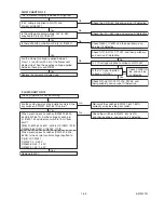
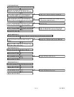
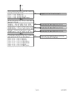
Are the analog audio signals outputted to each pin
of IC7201, IC7202 and IC7203?
IC7201 9,10PIN FRONT(L/R)
IC7202 9,10PIN SORROUND(L/R)
IC7203 9,10PIN CENTER/SUBWOOFER
IC7301 2, 6PIN FRONT(L/R)
IC7401 2, 6PIN SORROUND(L/R)
IC7501 2, 6PIN CENTER/SUBWOOFER
Is +5V voltage applied to the pin(8) of IC7201,
IC7202 and IC7203? And is +3.3V voltage applied
to the pin(7) of IC7201, IC7202 and IC7203?
Are the analog audio signals inputted to each pin
of IC7301, IC7401 and IC7501?
Check each line between each pin of IC7201,
IC7202, IC7203 and each pin of IC7301, IC7401
and IC7501, and service it if defective.
IC7201 9,10PIN
→
IC7301 2,6PIN FRONT(L/R)
IC7202 9,10PIN
→
IC7401 2,6PIN SORROUND(L/R)
IC7203 9,10PIN
→
IC7501 2,6PIN CENTER/SUBWOOFER
Yes
Yes
Yes
No
No
No
Replace ICs (IC7201,
IC7202 or IC7203).
Check P-ON+3.3V or P-ON+5V
line and service it if defective.
Содержание DV4400
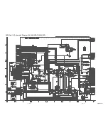
Страница 44: ...DVD Main 1 3 Schematic Diagram DV4400 N1B DV4400 N1S 1 8 3 1 8 4 E57M2SCD1 ...
Страница 45: ...DVD Main 2 3 Schematic Diagram DV4400 N1B DV4400 N1S 1 8 5 1 8 6 E57M2SCD2 ...
Страница 47: ...DVD Main 3 3 Schematic Diagram DV4400 N1B DV4400 N1S 1 8 9 1 8 10 E57M2SCD3 ...
Страница 49: ...AV 2 3 Schematic Diagram DV4400 N1B DV4400 N1S 1 8 13 1 8 14 E57M2SCAV2 ...
Страница 51: ...DVD Main 1 3 Schematic Diagram DV6400 N1B DV6400 N1S 1 8 17 1 8 18 E57M7SCD1 ...
Страница 52: ...DVD Main 2 3 Schematic Diagram DV6400 N1B DV6400 N1S 1 8 19 1 8 20 E57M7SCD2 ...
Страница 54: ...1 8 23 1 8 24 E57M7SCD3 DVD Main 3 3 Schematic Diagram DV6400 N1B DV6400 N1S ...
Страница 56: ...1 8 27 1 8 28 E57M7SCAV2 AV 2 3 Schematic Diagram DV6400 N1B DV6400 N1S ...
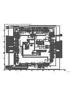
Страница 58: ...1 8 31 1 8 32 SACD 1 2 Schematic Diagram DV6400 N1B DV6400 N1S E57M7SCSA1 ...
Страница 59: ...1 8 33 1 8 34 SACD 2 2 Schematic Diagram DV6400 N1B DV6400 N1S E57M7SCSA2 ...
Страница 64: ...SACD CBA Top View DV6400 N1B DV6400 N1S 1 8 43 BE57D1F02011 1 8 44 ...
Страница 65: ...SACD CBA Bottom View DV6400 N1B DV6400 N1S BE57D1F02011 1 8 45 1 8 46 ...
Страница 73: ...1 13 3 E57M2EX X10 X2 X4 S2 S2 S4 Unit S1 X13 X1 X5 A22 Packing ...


