


1-3-2
DVD_SFNP
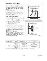
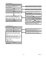
Chassis or Secondary Conductor
d
d'
Primary Circuit Terminals
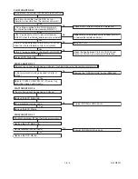
AC Voltmeter
(High Impedance)
Exposed Accessible Part
B
One side of
Power Cord Plug Prongs
Z
Safety Check after Servicing
Examine the area surrounding the repaired location for
damage or deterioration. Observe that screws, parts,
and wires have been returned to their original posi-
tions. Afterwards, do the following tests and confirm
the specified values to verify compliance with safety
standards.
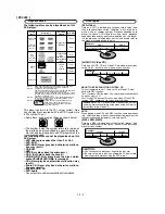
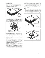
1. Clearance Distance
When replacing primary circuit components, confirm
specified clearance distance (d) and (d’) between sol-
dered terminals, and between terminals and surround-
ing metallic parts. (See Fig. 1)
Table 1 : Ratings for selected area
Note:
This table is unofficial and for reference only.
Be sure to confirm the precise values.
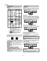
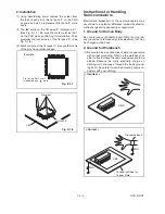
2. Leakage Current Test
Confirm the specified (or lower) leakage current
between B (earth ground, power cord plug prongs)
and externally exposed accessible parts (RF termi-
nals, antenna terminals, video and audio input and
output terminals, microphone jacks, earphone jacks,
etc.) is lower than or equal to the specified value in the
table below.
Measuring Method (Power ON) :
Insert load Z between B (earth ground, power cord
plug prongs) and exposed accessible parts. Use an
AC voltmeter to measure across the terminals of load
Z. See Fig. 2 and the following table.
AC Line Voltage
Clearance Distance (d) (d’)
230 V
≥
3 mm(d)
≥
6 mm(d’)
Fig. 1
Fig. 2
Table 2: Leakage current ratings for selected areas
Note:
This table is unofficial and for reference only. Be sure to confirm the precise values.
AC Line Voltage
Load Z
Leakage Current (i)
One side of power cord plug
prongs (B) to:
230 V
2k
Ω
RES.
Connected in
parallel
i
≤
0.7mA AC Peak
i
≤
2mA DC
RF or
Antenna terminals
50k
Ω
RES.
Connected in
parallel
i
≤
0.7mA AC Peak
i
≤
2mA DC
A/V Input, Output
Содержание DV4400
Страница 44: ...DVD Main 1 3 Schematic Diagram DV4400 N1B DV4400 N1S 1 8 3 1 8 4 E57M2SCD1 ...
Страница 45: ...DVD Main 2 3 Schematic Diagram DV4400 N1B DV4400 N1S 1 8 5 1 8 6 E57M2SCD2 ...
Страница 47: ...DVD Main 3 3 Schematic Diagram DV4400 N1B DV4400 N1S 1 8 9 1 8 10 E57M2SCD3 ...
Страница 49: ...AV 2 3 Schematic Diagram DV4400 N1B DV4400 N1S 1 8 13 1 8 14 E57M2SCAV2 ...
Страница 51: ...DVD Main 1 3 Schematic Diagram DV6400 N1B DV6400 N1S 1 8 17 1 8 18 E57M7SCD1 ...
Страница 52: ...DVD Main 2 3 Schematic Diagram DV6400 N1B DV6400 N1S 1 8 19 1 8 20 E57M7SCD2 ...
Страница 54: ...1 8 23 1 8 24 E57M7SCD3 DVD Main 3 3 Schematic Diagram DV6400 N1B DV6400 N1S ...
Страница 56: ...1 8 27 1 8 28 E57M7SCAV2 AV 2 3 Schematic Diagram DV6400 N1B DV6400 N1S ...
Страница 58: ...1 8 31 1 8 32 SACD 1 2 Schematic Diagram DV6400 N1B DV6400 N1S E57M7SCSA1 ...
Страница 59: ...1 8 33 1 8 34 SACD 2 2 Schematic Diagram DV6400 N1B DV6400 N1S E57M7SCSA2 ...
Страница 64: ...SACD CBA Top View DV6400 N1B DV6400 N1S 1 8 43 BE57D1F02011 1 8 44 ...
Страница 65: ...SACD CBA Bottom View DV6400 N1B DV6400 N1S BE57D1F02011 1 8 45 1 8 46 ...
Страница 73: ...1 13 3 E57M2EX X10 X2 X4 S2 S2 S4 Unit S1 X13 X1 X5 A22 Packing ...