1-6-2
E57M2TR
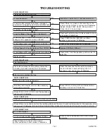
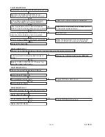
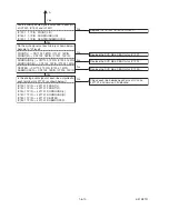
FLOW CHART NO.7
P-ON+5V is not outputted. (EV+9V is outputted normally.)
Is the "H" pulse inputted into the base of Q1004?
Replace Q1004.
Check R1068 and D1046, and service it if defective.
Yes
No
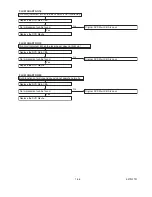
FLOW CHART NO.8
P-ON+3.3V is not outputted. (P-ON+12V is outputted normally.)
Is 3.3V voltage supplied to the collector of Q1011?
Replace Q1011 and R1067.
Check D1008, D1015, C1007, C1038, L1007 and
the periphery circuit, and service it if defective.
Yes
No
FLOW CHART NO.9
EV+5V is not outputted. (EV+9V is outputted normally.)
Is the "H" pulse inputted into the base of Q1014?
Replace Q1014.
Check Q1014, D1047 and the periphery circuit,
and service it if defective.
Yes
No
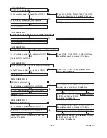
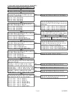
FLOW CHART NO.6
P-ON+12V is not outputted.
Is 14V voltage supplied to the emitter of Q1002?
Is the voltage of base on Q1002 lower than the
voltage of emitter on Q1002 when turning the power on?
Replace Q1002.
Check D1030, D1048, D1053, C1035, C1048, L1009
and the periphery circuit, and service it if defective.
Check Q1016 and PWRCON line and service it if
defective.
Yes
Yes
No
No
FLOW CHART NO.10
EV+1.5V is not outputted.
Is 2.5V voltage supplied to Pin(1) of IC1002?
Is 1.25V voltage supplied to Pin(4) of IC1002?
Replace IC1002.
Replace IC2002.
Check the circuit between Pin(19)
of IC2002 and Pin(4) of IC1002,
and service it if defective.
Check D1006, C1014, C1050, L1008 and the
periphery circuit, and service it if defective.
Is the "L" pulse outputted into Pin(19) of IC2002?
Yes
Yes
Yes
No
No
No
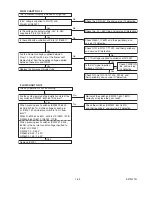
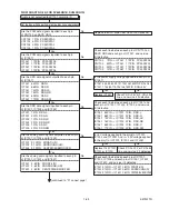
FLOW CHART NO.11
EV+3.3V is not outputted.
Is 3.3V voltage supplied to emitter of Q1010?
Is the "L" pulse inputted to base of Q1012?
Check Q1010, Q1012, R1087 and R1088, and
service it if defective.
Replace IC2002.
Check the circuit between Pin(19)
of IC2002 and base of Q1012,
and service it if defective.
Check D1008, D1015, C1007, C1038, L1007 and
the periphery circuit, and service it if defective.
Is the "L" pulse outputted into Pin(19) of IC2002?
Yes
Yes
Yes
No
No
No
Содержание DV4400
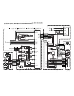
Страница 44: ...DVD Main 1 3 Schematic Diagram DV4400 N1B DV4400 N1S 1 8 3 1 8 4 E57M2SCD1 ...
Страница 45: ...DVD Main 2 3 Schematic Diagram DV4400 N1B DV4400 N1S 1 8 5 1 8 6 E57M2SCD2 ...
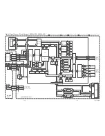
Страница 47: ...DVD Main 3 3 Schematic Diagram DV4400 N1B DV4400 N1S 1 8 9 1 8 10 E57M2SCD3 ...
Страница 49: ...AV 2 3 Schematic Diagram DV4400 N1B DV4400 N1S 1 8 13 1 8 14 E57M2SCAV2 ...
Страница 51: ...DVD Main 1 3 Schematic Diagram DV6400 N1B DV6400 N1S 1 8 17 1 8 18 E57M7SCD1 ...
Страница 52: ...DVD Main 2 3 Schematic Diagram DV6400 N1B DV6400 N1S 1 8 19 1 8 20 E57M7SCD2 ...
Страница 54: ...1 8 23 1 8 24 E57M7SCD3 DVD Main 3 3 Schematic Diagram DV6400 N1B DV6400 N1S ...
Страница 56: ...1 8 27 1 8 28 E57M7SCAV2 AV 2 3 Schematic Diagram DV6400 N1B DV6400 N1S ...
Страница 58: ...1 8 31 1 8 32 SACD 1 2 Schematic Diagram DV6400 N1B DV6400 N1S E57M7SCSA1 ...
Страница 59: ...1 8 33 1 8 34 SACD 2 2 Schematic Diagram DV6400 N1B DV6400 N1S E57M7SCSA2 ...
Страница 64: ...SACD CBA Top View DV6400 N1B DV6400 N1S 1 8 43 BE57D1F02011 1 8 44 ...
Страница 65: ...SACD CBA Bottom View DV6400 N1B DV6400 N1S BE57D1F02011 1 8 45 1 8 46 ...
Страница 73: ...1 13 3 E57M2EX X10 X2 X4 S2 S2 S4 Unit S1 X13 X1 X5 A22 Packing ...

