1-6-3
E57M2TR
Yes
No
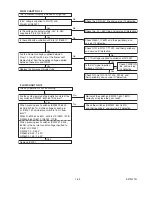
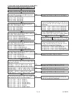
FLOW CHART NO.13
The key operation is not functioning.
Are the contact point and the installation state of the
key switches (SW2001, 6401-6413) normal?
When pressing each switches (SW6401-6403,
6405, 6407-6413), do the voltage of each pin
of IC6001 (shown below) switch to 75mV from
6mV?
SW6401-6403, 6405, 6407, 6409, 6413: IC6001 10PIN
SW6408, 6410-6412: IC6001 11PIN
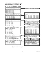
When pressing each switches (SW2001, 6404,
6406), is the normal control voltage inputted to
Pin(8) of IC2002?
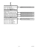
SW2001: 0 - 0.49V
SW6406: 0.49 - 1.49V
SW6404: 1.49 - 2.42V
Check the switches (SW2001, 6401-6413)
and their periphery, and service it if detective.
No
Re-install the switches (SW2001, 6401-6413)
correctly or replace the poor switch.
Replace IC2001.
Yes
Yes
Yes
Yes
Yes
No
No
No
No
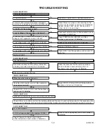
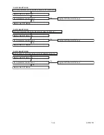
FLOW CHART NO.12
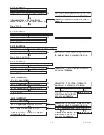
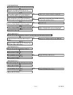
The fluorescent display tube does not light up.
Is 5V voltage supplied to Pin(13) and
Pin(43) of IC6001?
Is the voltage of approximately -24V to -28V
supplied to Pin(30) of IC6001?
Is there 500kHz oscillation at Pin(5) of IC6001?
Are the filament voltage supplied between
Pins(1, 2) and Pins(34, 35) of the fluorescent
display tube? And the negative voltage applied
between these pins and GND?
Replace the fluorescent display tube.
Check the P-ON+5V line and service it if detective.
Check the -FL (-28V) line and service it if detective.
Check R6001, IC6001 and their periphery, and
service it if detective.
Check PWRCON
line, and service
it if detective.
Is the "H" signal inputted
to base of Q1016?
Check D1016, D1017, T1001, and their periphery,
and service it if detective.
Is -17V voltage supplied to collector of Q1005?
No
Yes
Yes
No
Check Q1005, Q1015, Q1016, D1055, and
their periphery, and service it if detective.
Содержание DV4400
Страница 44: ...DVD Main 1 3 Schematic Diagram DV4400 N1B DV4400 N1S 1 8 3 1 8 4 E57M2SCD1 ...
Страница 45: ...DVD Main 2 3 Schematic Diagram DV4400 N1B DV4400 N1S 1 8 5 1 8 6 E57M2SCD2 ...
Страница 47: ...DVD Main 3 3 Schematic Diagram DV4400 N1B DV4400 N1S 1 8 9 1 8 10 E57M2SCD3 ...
Страница 49: ...AV 2 3 Schematic Diagram DV4400 N1B DV4400 N1S 1 8 13 1 8 14 E57M2SCAV2 ...
Страница 51: ...DVD Main 1 3 Schematic Diagram DV6400 N1B DV6400 N1S 1 8 17 1 8 18 E57M7SCD1 ...
Страница 52: ...DVD Main 2 3 Schematic Diagram DV6400 N1B DV6400 N1S 1 8 19 1 8 20 E57M7SCD2 ...
Страница 54: ...1 8 23 1 8 24 E57M7SCD3 DVD Main 3 3 Schematic Diagram DV6400 N1B DV6400 N1S ...
Страница 56: ...1 8 27 1 8 28 E57M7SCAV2 AV 2 3 Schematic Diagram DV6400 N1B DV6400 N1S ...
Страница 58: ...1 8 31 1 8 32 SACD 1 2 Schematic Diagram DV6400 N1B DV6400 N1S E57M7SCSA1 ...
Страница 59: ...1 8 33 1 8 34 SACD 2 2 Schematic Diagram DV6400 N1B DV6400 N1S E57M7SCSA2 ...
Страница 64: ...SACD CBA Top View DV6400 N1B DV6400 N1S 1 8 43 BE57D1F02011 1 8 44 ...
Страница 65: ...SACD CBA Bottom View DV6400 N1B DV6400 N1S BE57D1F02011 1 8 45 1 8 46 ...
Страница 73: ...1 13 3 E57M2EX X10 X2 X4 S2 S2 S4 Unit S1 X13 X1 X5 A22 Packing ...

