background image

LMS6002D Quick Starter Manual for Evaluation Board 

43 | 

P a g e


© Copyright Lime Microsystems


Rev: 2.2 
Last modified: 03/05/2012 


Figure 38 VCO Capacitance 


Use of the 

‘Calibration’

 button is described at the end of this section. 


Charge Pump(CP) Current and Offset 

CP  Current  and  Offset  is  set  based  on  the  selected  loop  filter  and  loop  BW.  For  the 
recommended loop filter (implemented on the evaluation board). Current should be 1200uA 
and Up Offset 30uA, as shown. 


Figure 39 CP Current and Offset  


PLL Calibration Data and File 

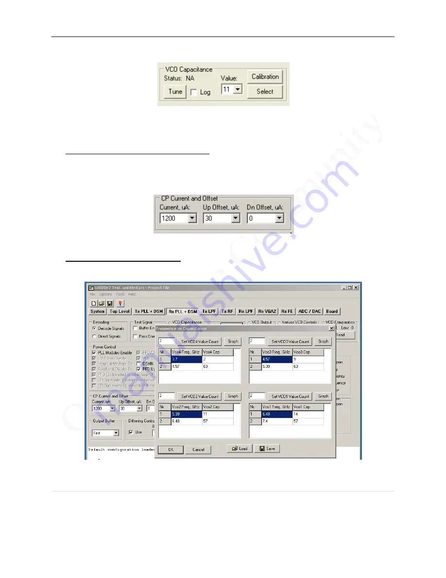
Press the 

‘Calibration’

 button to enter the Frequency vs Capacitance calibration table data. 


Figure 40 Frequency vs capacitance calibration table data 

Содержание LMS6002D

Страница 1: ...d The Surrey Research Park Guildford Surrey GU2 7YG United Kingdom LMS6002D Quick Start Manual The information contained in this document is subject to change without prior notice Lime Microsystems assumes no responsibility for its use nor for infringement of patents or other rights of third parties Lime Microsystems standard terms and conditions apply at all times ...

Страница 2: ...tor 16 3 3 Hardware options Clocking TCXO SPI 16 3 4 TCXO Frequency and Data Clocks Distribution 17 3 5 Different Clocking Schemes 18 3 6 TCXO Locking Options 19 3 7 SPI Control Options 20 4 Installing and Running PC Software Application 22 4 1 Windows XP Operating System 22 4 2 Determining Serial Port 25 4 3 Windows 7 Operating System 26 4 3 1 Determining Serial Port 27 4 4 Turn On and SPI Check ...

Страница 3: ...edures 66 6 1 TX LO Leakage Calibration 66 6 2 Transmit I Q Balance Calibration 69 6 3 Receiver DC Calibration 72 6 4 Calibration Process Summary 76 7 Appendix A Saving and Retrieving SPI Test Setups 77 7 1 Saving a Setup 77 7 2 Loading prj Files 78 8 Appendix B Test Systems Connections 80 8 1 Basic Setup 80 8 2 Transmitter Test System Connections 81 8 3 Receive Test System Connections 81 9 Append...

Страница 4: ...Figure 15 Check in device manager the new communication port 27 Figure 16 Power supply reading 28 Figure 17 Run ctr_6002dr2 program as an administrator 28 Figure 18 GUI communication settings 29 Figure 19 GUI register test 29 Figure 20 GUI register test log 30 Figure 21 GUI System window 31 Figure 22 GUI Top Level window 33 Figure 23 GUI TxPLL DSM window 35 Figure 24 PLL mode 36 Figure 25 Output F...

Страница 5: ...Figure 60 Setting Rx LPF to 7 MHz 62 Figure 61 Setting Rx VGA2 gain 62 Figure 62 Rx LNA and VGA1 settings 63 Figure 63 Rx PLL settings 64 Figure 64 Oscilloscope capture of 1 MHz I Q Sine wave outputs 65 Figure 65 Transmit Output 67 Figure 66 System Window Use Automated Calibration 67 Figure 67 Transmit Output After Calibration 68 Figure 68 Tx RF window 68 Figure 69 Transmit output after calibratio...

Страница 6: ...ast modified 03 05 2012 Figure 85 Transmitter test setup 81 Figure 86 Receiver test setup 81 Figure 87 Agilent N5181A 82A MXG Front Panel 82 Figure 88 Rx PLL VCO capacitance 89 Figure 89 No Receive Baseband Output 89 Figure 90 Non sinusoidal baseband Output 90 Figure 91 Sinusoidal Baseband Output 90 ...

Страница 7: ...as developed with best layout decoupling and matching practices to deliver optimum LMS6002D RF performance This document provides instructions on how to load the evaluation board software ctr6002d onto a PC connect the PC to the board control the LMS6002 via the ctr6002d software and evaluate its performance A summary of the main steps to complete this is shown below Install PC ctr6002d software C...

Страница 8: ...ied 03 05 2012 2 Development System Contents Before commencing any work please ensure all of the contents listed below are contained in the system shipped See Figure 1 Development System Contents below Figure 1 Development System Contents 5V Supply cable for LMS6002D Board PC to USB cable USB software stick ...

Страница 9: ...nded drivers on each of the receiver outputs to accommodate testing with an oscilloscope An interface via pin header J5 is provided to the parallel digital interface on the LMS6002D A baseband connector via pin header J2 is also provided to be used with third party basebands RX IN 1 is tuned from 700 1500 MHz to cover UMTS bands V and VIII whilst RX IN 2 is tuned from 1 5 2 5 GHz to cover UMTS ban...

Страница 10: ...rd 10 P a g e Copyright Lime Microsystems Rev 2 2 Last modified 03 05 2012 3 2 Board Connections Figure 2 Evaluation board connection descriptions The following table describes the high level pin assignment for each connector on the evaluation board ...

Страница 11: ...tor the signal in full operation mode The transmit input signals required are differential I and Q The Receiver signals have both single ended and differential outputs Single ended provided for test purposes J4 CLK I O Clock input for locking the external clock from test equipment to the Lime on board clock J4 connector is used to supply the on board ADF4002 board clock PLL device with 10 MHz cloc...

Страница 12: ...nput RX3 input direct to chip J14 TX OUT 1 Transmitter output TX1 output direct from the chip J16 USB USB Connector to PC Table 1 Evaluation board connectors 3 2 1 J1 Main Power Supply Connector Figure 3 Connector J1 circuit diagram For standard mode Pin1 or Pin2 is connected to external power supply up to 5V Pin 3 or Pin4 is connected to ground ...

Страница 13: ...used by third party baseband providers Figure 4 Connector J2 circuit diagram The SAM QSS RA 150 is a standard connector used by third party baseband providers The LMS6002D board is shipped configured to operate using the connector J5 in standalone mode The board has been fitted with several 0 Ω resistors which act as links to configure the board in different ways depending on which baseband board ...

Страница 14: ...3 05 2012 3 2 3 J3 Analogue IQ Signals Figure 5 Connector J3 circuit diagram Pins 18 and 20 of J3 connector are single ended analogue receiver outputs Pins 10 12 14 and 16 are differential analogue receiver outputs Pins 2 4 6 and 8 are differential analogue transmitter inputs All other pins are ground connections ...

Страница 15: ...I O I Q TX 12 Bit TXIQSel and RX 12 Bit RXIQSel Figure 6 Connector J5 circuit diagram The digital I Q connector is a digital transmit TX and receive RX interface to the ADC DAC of the LMS6002D The SPI can be controlled within the J5 connector J5 can also be used as a test connector when the board is connected to a third party baseband board ...

Страница 16: ...tribution Section 3 4 TCXO Locking method Section 3 6 SPI connection options Section 3 7 The default mode the board is shipped with means basic operation using an external digital I O source via connector J5 digital I O I Q TX 12 Bit Select and RX 12 Bit Select Various options are available depending on the system configuration required for testing or development work The options are summarized be...

Страница 17: ...30 72MHz output TX data clock is provided by Lime evaluation board and is fed to connectors J2 J5 as outputs to enable a digital I O card to send samples Option 2 Description PLL clock 30 72MHz TCXO 2 LMS6002D device PLL is fed using on board TCXO 61 44MHz clock 2 Rx data clock 61 44MHz output RX data clock is provided by Lime evaluation board and is fed to connectors J2 J5 as outputs to enable a ...

Страница 18: ...k 30 72 MHz TCXO 30 72 MHz TCXO 30 72 MHz TCXO Rx data clock 30 72 MHz output 61 44 MHz output Input from digital I O card Tx data clock 30 72 MHz output 30 72 MHz output Input from digital I O card Evaluation Board Component fit option 1 Component fit option 2 Component fit option 3 R81 NF NF 0R R80 NF 0R 0R R104 NF NF NF R105 0R 0R NF R106 0R NF NF R107 68R NF 68R R111 NF 0R NF R113 0R 0R 0R R11...

Страница 19: ...rd potentiometer J4 becomes an output for the reference clock Option 3 External control via the baseband connector J2 Signal VCTRL provided by baseband board The board is shipped in the default mode Option 1 To use other options please use component changes as in table below Please note that NF denotes component is not fitted TCXO Locking method Options Option 1 DEFAULT MODE On Board PLL Clock ADF...

Страница 20: ...hence these are mutually exclusive The only option requiring hardware changes is Option 2 where the baseband connector J2 is used to connect to a baseband board for the TX RX signals when its own SPI bus and control of the SPI by the Lime SW is desired rather than the BB SPI J2 must be removed from the EVB SPI bus so that the control of the SPI is maintained by a PC running the Lime software This ...

Страница 21: ...baseband SPI disabled Used with 3rd party baseband boards and controlling LMS6002D with PC S W via USB Description SPI connected to PC via USB connector J16 SPI connected to BB via connector J2 SAMTEC Component R133 NF 0R R134 NF 0R R135 NF 0R R136 NF 0R R137 NF 0R Table 5 SPI Control Options All of these components are located on the underside of the board and can be located using the diagram bel...

Страница 22: ... Windows XP Operating System Plug USB cable to USB port of the interface board 1 You will need to be logged in as Administrator to the free USB port on your Windows machine 2 No external power connection is required After plugging in the board Windows New Hardware Wizard should appear After installation procedure begins DO NOT let Windows search as it will not find anything ...

Страница 23: ...e 10 Hardware wizard Next you will want to install from a specific location Figure 11 Hardware wizard Install driver manually Next you need to point to the USBDriver inf file which can be found in the QuickStarterKit folder Use the browse function to find this file The same file for Windows XP and Windows Vista should work fine ...

Страница 24: ...ied 03 05 2012 Figure 12 Hardware wizard Choose the USBDriver inf from the folder Windows should proceed to install drivers Enumeration process USB term meaning connect and establish communication with should start now If everything is successful unplug and then plug in your device again to be able to use it ...

Страница 25: ...ning connect and establish communication with Windows will assign to your USB Virtual Serial device a serial port COM Right Click on My Computer then click Properties then the Hardware tab then Device Manager then find USB Virtual Serial Port under Ports COM LPT Note that in this system example it has enumerated as COM3 Figure 13 Check in device manager the new communication port ...

Страница 26: ...vices 3 Right click on LUFA USB RS232 Demo icon 4 Click on Update Driver Software and select 2nd option Browse my computer for driver software Locate and install driver software manually as shown below Figure 14 Device Manager Choose the USBDriver inf from the folder 5 The folder should point to the USBDriver inf file which can be found in the QuickStarterKit folder Use the browse function to find...

Страница 27: ...ng connect and establish communication with Windows will assign to your USB Virtual Serial device a serial port COM Click on Control Panel then click System and Security then click System then click Device Manager then find USB Virtual Serial Port under Ports COM LPT Note that in this system example it has enumerated as COM4 Figure 15 Check in device manager the new communication port ...

Страница 28: ...oximately 0 15A on the power supply 0 15 Figure 16 Power supply reading Start LMS6002D board control S W located in QuickStarterKit transferred from the Lime USB stick The SPI APP picture of ICON is shown below Note For Window 7 operating system right click on the ctr_6002dr2 exe icon above Next click on Properties and click on the Compatibility tab as shown below Figure 17 Run ctr_6002dr2 program...

Страница 29: ...e following window appears Figure 18 GUI communication settings Select enumerated port under USB board In this case it is COM4 but port may be different Choose desired SPI clock frequency and push OK Now you are able to communicate with the LMS6002D test board using USB to Serial adapter To check this is working select the register test sequence by going to menu Tools Register Test Figure 19 GUI r...

Страница 30: ...tween the PC and the evaluation board USB port You will need to check connection and start the process again If the system test returns FF then you know the PC and the USB port are communicating properly Connect the Lime board to 5V supply and start the process again If you now get an OK for the register test map results then the system is ready for testing If the system still returns 00 or FF ins...

Страница 31: ...page allows configuring the synthesizers to the 3GPP bands by channel number and has buttons for bottom middle and top frequencies for each This makes changing frequency for the commonly used test channels simpler Automatic calibration the calibrations the device carries out itself under SPI prompting is also done from this page Figure 21 GUI System window Downlink and Uplink Frequency setting by ...

Страница 32: ...per device to ensure that the corner frequencies of the LPFs are optimized The calibration selects the LPF response which is closest and above the required bandwidth This ensures modulation quality is not adversely impacted but sufficient rejection is provided for adjacent and alternate channel attenuation This should be done 1st as optimum DC calibration values for LPF s will change if this is do...

Страница 33: ...the top level DC calibration for the device this is the R component of the RC cal value which is used in each of the LPF Tx and Rx process calibration values Only calibration module address 0 is used Clock Buffers control Enable pins turn the internal clock buffers on and off These should be enabled when control of the device is needed however during operation SPI clocks which are not being used s...

Страница 34: ... to execute the calibration The result can be found in the DC calibration area when the read button is pressed Enable Enforce Mode and LPFCAL Code are not used LPF BW sets the bandwidth used for the calibration If you are using WCDMA select 2 5MHz The result should be copied into the TXLPF and RXLPF from TRX_LPF_CAL drop down box Decoding Select Decode Signals or Direct Signals for control of diff...

Страница 35: ... diagram below are enabled Figure 23 GUI TxPLL DSM window Description of each function available from this page is as follows Decoding Select Decode or Direct signals for control of different parts of the SPI memory map When swapping between the two options the available options are highlighted and the unavailable ones grayed out Use Decode mode Dithering Control DSM dithering Leave it set to 1 Po...

Страница 36: ...ol not used in TxPLL Frequency Control Sets the PLL divide ratios VCO and output divider selection The individual parts of this block are described in more detail below PLL Mode selects fractional or integer mode Use fractional mode Figure 24 PLL mode Output Frequency GHz set the desired Tx LO frequency in the text box Calculate button calculates the required divide ratio based on the required LO ...

Страница 37: ...es for Fractional Mode To properly select the VCO Capacitance click Tune after Calculate If you want to observe the VCO capacitor selection algorithm results select Log Figure 27 VCO Capacitance The Current VCO and the MUX DIV Selection show the choice made by pressing Calculate or Tune buttons see below Figure 28 Current VCO and MUX DIV selections ...

Страница 38: ...nce click Tune after Calculate If you want to observe the VCO capacitor selection algorithm results select Log Figure 29 VCO Capacitance Use of the Calibration button is described at the end of this section Charge Pump CP Current and Offset Figure 30 CP Current and Offset CP Current and Offset is set based on the selected loop filter and loop BW For the recommended loop filter implemented on the e...

Страница 39: ...data If not file Dr2 vco provided with SW should be loaded To load a new VCO file press the Load button and follow the normal windows procedure to load a file Then press OK This new file will now be downloaded on subsequent starts of the software 4 5 4 Rx PLL DSM The Rx PLL is controlled from this page if the frequency control on the System Interface page is used and the correct set up files have ...

Страница 40: ... signals for control of different parts of the SPI memory map When swapping between the two options the available options are highlighted and the unavailable ones grayed out Use Decode mode Dithering Control DSM dithering Leave it set to 1 Power Control Individual parts of the PLL circuitry can be turned on and off leave as default Test Signal Design test signals leave unchecked VCO Comparators Re...

Страница 41: ...rd and Disable Selection of LNA in tool on System page automatically selects the correct buffer Frequency Control Sets the PLL divide ratios VCO and output divider selection The individual parts of this block are described in more detail below PLL Mode selects fractional or integer mode Use fractional mode Figure 33 PLL Mode Output Frequency GHz set the desired Tx LO frequency in the text box Calc...

Страница 42: ...citance The Current VCO and the MUX DIV Selection show the choice made by pressing Calculate or Tune buttons see below Figure 37 Current VCO and MUX DIV selections VCO Capacitance Correct setting of VCO capacitance is described in LMS6002D Programming and Calibration Guide Selections made when using the Calculate button however are decided based on the calibration table used in this block To prope...

Страница 43: ...mp CP Current and Offset CP Current and Offset is set based on the selected loop filter and loop BW For the recommended loop filter implemented on the evaluation board Current should be 1200uA and Up Offset 30uA as shown Figure 39 CP Current and Offset PLL Calibration Data and File Press the Calibration button to enter the Frequency vs Capacitance calibration table data Figure 40 Frequency vs capa...

Страница 44: ...on subsequent starts of the software 4 5 5 Tx LPF The Tx LPF page contains the SPI controls for the transmitter low pass filters notably the LPF BW and also the controls for the DC calibration Figure 41 Tx LPF page Description of each function available from this page is as follows DC Calibration These are the individual controls for the DC correction and auto calibration routines for the TX LPF c...

Страница 45: ...ss trim the LPF BW Values are calculated in top level calibration and written into these locations carried out automatically by LPF Core on System page Decoding Select Decode or Direct signals for control of different parts of SPI memory map When swapping between the 2 options the available options are highlighted and the unavailable ones are grayed out Decode mode is recommended 4 5 6 Tx RF The T...

Страница 46: ...dB via drop down box VGA1 Gain Test sets VGA1 gain in Direct Signals mode by setting 8 bit not log linear control word directly LO Leakage I DAC Out and LO Leakage Q DAC Out set DC level injected via the LO correction DACs for LO cancellation VGA2 Control VGA2 Gain sets VGA2 gain RF gain stage from 0 to 25dB via drop down box VGA2 Gain Test set VGA2 gain in Direct Signals mode by setting 9 bit not...

Страница 47: ...cessed by using direct signals mode Using Decode mode is recommended LPF Bandwidth Set the LPF BW in the drop down box from 0 75MHz to 14MHz Note that RF system BW is twice this number i e 0 75MHz LPF BW is 1 5MHz system BW Test LPF bypass for test purposes Ensure Normal Operation is enabled Process Calibration Values RC calibration values used to process trim the LPF BW values are calculated in t...

Страница 48: ...libration routines for the RX VGA2 controlled by the Receiver auto calibration button on the System page The Rx VGA2 DC calibration has 5 stages which can be calibrated RXVGA2 Top at Cal module address 0 RXVGA2a I at Cal module address 1 RXVGA2a Q at Cal module address 2 RXVGA2b I at Cal module address 3 RXVGA2b Q at Cal module address 4 Decoding Select Decode or Direct signals for control of diff...

Страница 49: ...use VGA2B Gain Test and VGA2A Gain Test are available in test mode to control A and B stages directly Decoding is set to Direct Signals to use this function This feature is not used for normal operation VGA2 CM Voltage Sets RXVGA2 output common node voltage to interface to ADCs Code 12 which corresponds to 780mV is recommended 4 5 9 RX FE Sets the SPI controls for the RX Front End stages including...

Страница 50: ...2 Cancellation Applies offset to mixer to improve IP2 performance Not required LNA Control Settings for LNA controls are as follows Internal External LNA load tick boxes use internal Capacitance to BE leave as default 0 LNA Gain Mode selects LNA gain Max Mid and Bypass LNA3 Fine Gain fine gain setting for LNA3 which has no bypass mode 0 to 3dB Active LNA Select active LNA 1 to 3 also need to chang...

Страница 51: ...lt See figure below for settings Figure 47 MIX Control settings VGA1 Control Feedback Resistor 0 to 123 Only use settings up to 120 Sets VGA1 gain max 0dB 120 min 24dB 0 so do not set above 120 Gain control is not log linear Feedback capacitor 0 to 123 Introduces a single pole LPF at VGA1 output Bandwidth dependent on Feedback resistor and Feedback capacitor For no filtering leave at default 0 Bia...

Страница 52: ...fferent parts of the SPI memory map When swapping between the two options the available options are highlighted and the unavailable ones are grayed out ADC DAC Miscellaneous Control Rx Fsync Polarity sets the polarity of the RX IQ SEL signal for the first sample of the Rx IQ pair Rx Interleave sets the order of the RX IQ pair Tx Fsync Polarity sets the polarity of the TX IQ SEL signal for the firs...

Страница 53: ... the data is clocked from Negative is usually required ADC DAC Enable Control Check ADC Enable to enable ADCs and DACs Sub blocks are also independently controllable in Direct Signals mode DAC Control Internal output Load Resistor 50 66 100 200 Ohms or Open Circuit setting when using external load resistor DAC Reference Current resistor use External DAC Full Scale Output Current 2 5 5 10mA Use Loa...

Страница 54: ...as Res Adj 10uA minimizes ADC noise Common mode Adj 960mV Ref Gain Adj 1 75V See diagram below for settings including the exceptions listed above which have been highlighted in red Figure 52 ADC Control settings 4 5 11 Board Board refers to the interface board This page provides the SPI control via a second enable pin on the SPI interface for an external PLL chip The purpose of this is so the inte...

Страница 55: ...he default settings will program the standard board with a 30 72MHz TCXO and a 10MHz reference Using this feature Press Download All ADF4002 Configuration button Then Press Calculate R N Download button to program the ADF4002 if all is correct the green PLL locked LED LD1 on the interface board should illuminate LD1 is located in the upper left hand corner of the interface board ...

Страница 56: ... Tx chain for accurate repeatable measurements the Baseband Interface data DACs should be set to a known state Also verify the reference clock frequency is set properly The reference clock frequency can be set in the top Options menu under Reference Clock It is typically set to 30 72 MHz but can vary depending upon the frequency of the TCXO installed on the evaluation board 5 1 1 Top Level Setting...

Страница 57: ...tings Note The LMS6002 communication can be easily checked by toggling the Soft Tx Enable in the Power Control section The current change can be observed on power supply display 5 1 2 TX LPF Gain Setting Using the Tx LPF page Set the LPF bandwidth to your desired value see figure below example setting is 14 MHz Figure 55 Setting Tx LPF bandwidth ...

Страница 58: ...PA selection 5 1 3 TX PLL Setup Select Tx PLL DSM page to set up the Tx PLL Please follow the instructions 1 to 3 below in the order shown and illustrated in the figure below 1 Set Output frequency Tx frequency example shown 2 14GHz and then press Calculate note divider ratios should change 2 Change CP Current and Offset CP Charge Pump to the following a Current uA 1200uA b Up offset uA 30uA 3 Pre...

Страница 59: ... your selected TX output can be connected to spectrum analyzer SA In SA you can now observe the results of this basic operational test The test is looking at the DC offset from the un programmed data DAC as LO leakage and the example shown below is measuring a value of 2 1dBm As the DACs are not programmed yet levels may be different from the screen shot example Figure 58 Basic TX testing using DC...

Страница 60: ... four tests are recommended TX RF VGA 1 change setting from 4 to 35 and observe results LO should vary by approx 1 dB steps 31dB range TX RF VGA 2 change setting from 0 to 25 and observe results LO should vary by approx 1 dB steps 25 dB range Change frequency from 2 14GHz to 2 11 GHz and press Calculate Tune CAP value should change check Spectrum Analyzer Change frequency from 2 11GHz to 2 17 GHz ...

Страница 61: ... checks on the receiver side are achieved by using the analogue output from connector J3 not using the digital output from the data ADCs 5 3 1 Top Level Settings Using the Top Level page verify the Rx DSM SPI Clock Buffers and the Soft Rx Enable Power Control is enabled in the menus as shown below Also verify the RxOut ADC in Switch is set to Closed Figure 59 Top Level Settings ...

Страница 62: ...gure 60 Setting Rx LPF to 7 MHz Select Rx VGA2 page to set the gain For basic operation set VGA2 gain 30 See figure below Figure 61 Setting Rx VGA2 gain Select RX FE page check VGA1 Control Feedback Resistor is set to 120 Default setting The feedback resistor controls the gain of VGA1 Set LNA gain by using LNA load resistor Internal load set to 55 Check Active LNA LNA1 and LNA Gain Mode is set to ...

Страница 63: ...elow in the order shown and illustrated in the figure below a Set Output Frequency Tx frequency example shown 1 95GHz and then press Calculate note divider ratios should change b Change CP Current and Offset CP Charge Pump to the following a Current uA 1200uA b Up offset uA 30uA c Press Tune to fine tune VCO capacitance If you want to observe the VCO capacitor selection algorithm results select Lo...

Страница 64: ...LMS6002D Quick Starter Manual for Evaluation Board 64 P a g e Copyright Lime Microsystems Rev 2 2 Last modified 03 05 2012 Figure 63 Rx PLL settings 2 1 3 ...

Страница 65: ...apture of 1 MHz I Q Sine wave outputs 5 4 1 RX Basic Operation Checks To check basic Rx frequency and gain control conduct some tests changing frequencies and gain settings The following six tests are recommended a RX VGA2 VGA 2 change setting from 30 to 0 observe results gain should decrease b RX FE VGA 1 change feedback resistor from 120 to 0 observe results gain should decrease c RX FE LNA gain...

Страница 66: ...le point calibration per band the example given uses 3GPP Band I with a centre frequency of 2140 MHz The transmitter should be set up with the following parameters Parameter Page Value Transmitter Frequency System Interface 2140 Soft Tx enable Top Level tick box selected Tx DSM SPI clock buffer Top Level Tick box selected LPF bandwidth Tx LPF 3 5MHz PA1 selected Tx RF PA1 Selected VGA1 gain Tx RF ...

Страница 67: ...resents the LO feedthru from the transmit modulator In this case the level is 45dBm Figure 65 Transmit Output Assuming the LPF Core calibration has been carried out in the initialisation then press the Transmitter button on the System Interface page in the Automatic Calibration area Figure 66 System Window Use Automated Calibration Tx Calibration Done should appear in the text box in bottom of the...

Страница 68: ...t just makes the DC contribution from the IQ chain as low as possible It may be the case that the level will go up after automatic calibration do not worry if it does this is due to the default values on power up cancelling the LO at the selected frequency Figure 67 Transmit Output After Calibration Select the Tx RF page in the SPI software Figure 68 Tx RF window The LO cancellation DACs level is ...

Страница 69: ... Do same for Q d It is possible that 0 is the best result for both as the optimum has been found during the LPF calibration above In this case the LO cancellation has been improved to 71dBm as shown in this figure The optimum values were I 0 Q 0 125 Figure 69 Transmit output after calibration 6 2 Transmit I Q Balance Calibration This procedure assumes the TX LO calibration procedure in section 6 1...

Страница 70: ... the test equipment cables and of course the LMS6002D transmit path The closer in length the cables between the signal generator and the test board are the better The phase match also depends on the accuracy of the sin cosine split on the LO of the IQ modulator inside the LMS6002D the bulk of the phase correction is for this parameter hence amplitude mismatch will vary little with frequency howeve...

Страница 71: ...ed as shown below The transmit I Q balance calibration is valid on the flat part of the LPF bandwidth As you approach the LPF corner frequency the lower sideband cancellation will begin to degrade For example with the 1 MHz tone used in this calibration the EVM will degrade as the filter bandwidth decreases below 1 92 MHz Figure 72 Amplitude balance calibration Using the VSA analysis software WCDM...

Страница 72: ... spectrum analyser but low DC levels are more difficult to measure In most cases the baseband BB processor is capable of adjusting the DC calibration and also the IQ phase and amplitude match based on measurements of the uplink signal It is only necessary to ensure the calibration is good enough so the ADC is not at full scale However for testing without the BB the following procedure has been dev...

Страница 73: ...t Lime Microsystems Rev 2 2 Last modified 03 05 2012 3 In Rx LPF Tab press Reset Calibration 4 In Rx VGA2 Tab Press Reset Calibration Figure 76 Rx VGA2 Tab DC Leakage after Calibration Reset DC offset very large would prevent automatic DC calibration Figure 75 Rx LPF tab ...

Страница 74: ...eceiver LO leakage 5 RXVGA1 Offset Optimisation In RX FE tab slightly adjust the RXVGA1 DC offset values to reduce the DC offset 6 Automatic DC Calibration If RX VGA1 DC Offset is small enough automatic DC calibration can be used in System Interface select receiver automatic calibration Figure 78 Rx VGA1 DC Offset Adjust in RX FE Tab ...

Страница 75: ...LMS6002D Quick Starter Manual for Evaluation Board 75 P a g e Copyright Lime Microsystems Rev 2 2 Last modified 03 05 2012 Figure 79 Rx automatic DC calibration result ...

Страница 76: ...ation can find the correct minimum DC point This DC calibration process provides optimum transmitter performance In the receiver a similar DC calibration process is applied but in reverse order When no signal is applied at the input of the receiver the resulting DC offsets at the receiver outputs are due to LO leakage multiplied by the RX gain and the DC offsets in the LPFs and VGAs The first step...

Страница 77: ...Saving and Retrieving SPI Test Setups The LMS6002D chip set up can be stored in a prj file and used in the future The Save Project feature of the software tool allows all the SPI settings to be saved for future use 7 1 Saving a Setup To save the SPI setup being used press the File button on the toolbar Select Save Project as shown below ...

Страница 78: ...luation Board 78 P a g e Copyright Lime Microsystems Rev 2 2 Last modified 03 05 2012 Figure 80 Save Project feature 7 2 Loading prj Files A prj file can be loaded using the standard windows procedure as shown below Figure 81 Open project ...

Страница 79: ...abled by the Options menu as shown below Figure 82 Auto Download feature If Auto Download is not enabled then the whole SPI map can be sent to the chip by using the download button as shown below Figure 83 Download Button for Previously Saved Setup Note The Ref clock frequency is not strictly part of the SPI information it is used to calculate the divider ratios for the PLLs When you start the sof...

Страница 80: ... Basic Setup Figure 84 Test system connections for receive and transmit Testing Signal Generator Oscilloscope 5V DC TX I Q Power Supply SPI TRX Control Uplink and downlink test models RX 1 RF TX 1 RF Spectrum Analyser VSA RX I Q Single ended TX LMS600 2 Test Board PC Laptop FTP file transfer Lime TRX Control S W Ethernet Ethernet VSA S W Signal Studio RX DC Block ...

Страница 81: ... 81 P a g e Copyright Lime Microsystems Rev 2 2 Last modified 03 05 2012 8 2 Transmitter Test System Connections Figure 85 Transmitter test setup 8 3 Receive Test System Connections Figure 86 Receiver test setup MS06054A MXA N9020A MS06054A MXA N9020A ...

Страница 82: ...l generator with an arbitrary waveform generator and the differential I Q outputs option 1EL Other signal generators can be used However some issues may arise if the options available for IQ amplitude and phase manipulation which come with the MXG are not supported 9 1 Agilent MXG Setup The front panel of the MXG is as follows Figure 87 Agilent N5181A 82A MXG Front Panel 1 2 3 4 5 23 Modes 24 I Q ...

Страница 83: ... section should alternate between on and off when pressed iii press return iv Check text next to I Q softkey 3 softkey 1 highlights off on v If not press I Q softkey 3 softkey 1 highlighted section should alternate between on and off when pressed There should now be a 0 6V common mode voltage on the differential IQ connections on the signal generator This can be verified by measuring the DC level ...

Страница 84: ...nal generator follow process described in 9 2 section To apply the correct file 1 Press Mode button 23 2 Press Dual Arb softkey 3 softkey 1 3 Press Select waveform softkey 3 softkey 2 4 Use up down arrows 5 or spin knob 18 to select wanted waveform from list 5 Press Select waveform softkey 3 softkey 1 6 Name of selected waveform should now be present in display window 7 Soft key list should have m...

Страница 85: ...lluminated a Press Mod on off button to toggle modulation on and off Note Mod on off button turns modulation on to RF output and IQ output simultaneously RF does not need to be on for IQ outputs to work 9 2 Downloading wfm Files to the Signal Generator The following process should allow you to download files to the Agilent signal generator The same process works for MXG and ESG This can be done vi...

Страница 86: ...and Prompt To check connection to signal generator attempt to ping it o Type ping 134 40 41 112 or use your sig gen IP address A successful ping result should be returned as shown below To send wfm files to signal generator the following procedure should be followed Ensure wfm files are in a known directory e g C Documents and Settings User My Documents wfm In Command Prompt window set directory t...

Страница 87: ... above should be returned Press return twice for user name and password none needed Type cd bbg1 Type cd waveform Type bin Type put wcdma31 wfm Applied command copies files to sig gen repeat put command for all files needed To exit the ftp program type bye To close Command Prompt window type exit The wfm files should now be visible in the list of Arb files ...

Страница 88: ...t all available frequencies This can be verified with a spectrum analyzer by checking to see if the VCO LO leakage signal is on frequency and phase locked Connect the spectrum analyser to the evaluation board J12 connector Set receiver input LNA2 and RxPLL for 1950 The VCO leakage signal will be at 2 x LO frequency Example Frx 1951MHz the VCO 2x1951MHz 3902 MHz However if the correct files have be...

Страница 89: ...will collapse but the box remains highlighted The up down arrows on the keyboard can now be used to cycle through the capacitance values As soon as the number is change it is downloaded to the LMS6002D so scrolling through and observing the effect is quite fast There are 3 types of display on the scope that can occur when doing this testing 1 No receive baseband output as shown below This implies ...

Страница 90: ... to the desired VCO capacitor value Figure 90 Non sinusoidal baseband Output 3 Locked PLL As shown below a sine wave at the difference between the CW RX input frequency and the LO frequency should be observed if the synthesizer locks at the desired in band frequency and the DC offset is calibrated There are some rules of thumb which may help in the process If all capacitor values are tried and onl...

Страница 91: ...ally obtained in the middle of the range Please note this is a problem solving procedure and these are rules of thumb but not comprehensive rules The provided VCO calibration files should set up the synthesiser properly If assistance is needed please contact Lime so the root problem with the SPI application software can be found 10 2 Is the Correct LNA Selected If the lower level pages of the SPI ...

Отзывы: