background image

LG-

K

D3500 


LGE


LG Electronics Inc.

     12/21 

5. Installation 


5.1 Installing a Battery Pack (Soft Pack type) 


1) The soft battery pack is keyed so it can only fit one way. Align the groove in the battery pack with 

the rail on the back of the phone until the battery pack rests flush with the back of the phone. 

2) Insert the bottom of battery into the openning on the back of the phone. Then, push the battery 

cover up until the latch clicks. 


5.2 For Adapter Use 


1) Plug the adapter into a wall outlet. The adapter can be operated from either a 110V or a 220V 

source. 

2) Insert the adapter jack into the phone with the installed battery pack. 

Red light indicates battery is being charged. Green light indicates battry is fully charged 


5.3 For Mobile Mount 


5.3.1 Installation Position 


In order to reduce echo sound when using the Hands-Free Kit, make sure that the speaker and 

microphone are not facing each other and keep microphone a generous distance from the speaker. 


5.3.2 Cable Connections 


5.3.2.1 Power and Ignition Cables 

Connect the red wire to the car battery positive terminal and the black wire to the car ground. Connect 

the green wire to the car ignition sensor terminal. ( In order to operate HFK please make sure to 

connect green wire to ignition sensor terminal.) Connect the kit’s power cable connector to the 

interface box power receptacle. 


5.3.2.2 Antenna Cable Connection 


Connect the antenna coupler cable connector from the cradle to the external antenna connector. ( Antenna is not 

included.) 


Содержание RD3500

Страница 1: ...ng the key board channel 5 Voltage and Current Value of Termination Part Amplifier Catalogue included Mode Type Name Voltage Current Power CDMA SKY77162 3 4V 455mA 0 282W 6 Functions of Major Semi Conductors Classification Function QSC6010 MSM baseband radioOne RF and power management MCP PF38F2040W0YBQ0 Flash Memory 64Mbit Storing of the mobile station operation program MCP PF38F2040W0YBQ0 PSRAM ...

Страница 2: ...CDMA MOBILE SUBSCRIBER UNIT LG KD3500 SINGLE BAND CDMA MOBILE PHONE SERVICE MANUAL ...

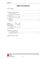
Страница 3: ...antages of CDMA Mobile Phone 5 3 Structure and Functions of CDMA Mobile Phone 8 4 Specification 9 5 Installation 12 CHAPTER 2 NAM Input Method Inputting of telephone numbers included 1 Telephone Number and NAM Programming Method 13 CHAPTER 3 Circuit Description 1 RF Transmit Receive Part 14 2 Digital Voice Processing Part 18 CHAPTER 4 BGA IC Pin Check ...

Страница 4: ...s are combined into this phone to reduce the call being interrupted in a middle of talking over phone CDMA digital cellular network consists of MSC Mobile Switching Office BSC Base Station Controller BTS Base station Transmission System and MS Mobile Station Communication between MS and BTS is designed to meet the specification of TIA EIA IS 95 A B C Common Air Interface MS meets the specification...

Страница 5: ...ain distance The analog cellular systems are classified further into an AMPS system E AMPS System NMT system ETACS system and JTACS system depending on technologies used Unlike the Time Division Multiple Access TDMA or the Frequency Division Multiple Access FDMA used in the band limited environment the Code Division Multiple Access CDMA system which is one of digital cellular systems is a multi ac...

Страница 6: ...me area several CDMA signals are overlapped Among these types of signals only desired signal energy is selected and received through the use of pre determined binary sequence desired signals can be separated and then received with the correlator used for recovering the spectrum into its original state At this time the spectrums of other signals that have different codes are not recovered into its ...

Страница 7: ...rom a base station to mobile stations and backward from the mobile station to the base station power control in order to increase the call processing capacity and obtain high quality calls In case the originating signals of mobile stations are received by the cell site in the minimum call quality level signal to interference through the use of transmit power control on all the mobile stations the ...

Страница 8: ... is selected for use depending on inputted automatic conditions and message data both of them utilize four stage frames of 9600 4800 2400 and 1200 bits per second In addition this type of variable voice encoder utilizes adaptive threshold values when selecting required data rate It is adjusted in accordance with the size of background noise and the data rate is increased to high rate only when the...

Страница 9: ...he same cell site about 65 In the case of directional cell site one cell normally uses a 120 sector antenna in order to divide the sector into three In this case each antenna is used only for 1 3 of mobile stations in the cell site and accordingly interference is reduced by 1 3 on the average and the capacity that can be supported by the entire system is increased by three times 2 7 Soft Capacity ...

Страница 10: ... symbols During the operation with one cell site the searcher searches out multi paths in accordance with terrain and building reflections On three data receivers the most powerful four paths are allocated for the parallel tracing and receiving Fading resistance can be improved a great deal by obtaining the diversity combined output for de modulation Moreover the searcher can be used to determine ...

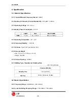
Страница 11: ... 580 mA 25dBm 4 1 5 Operating Temperature 30 60 4 1 6 Frequency Stability 0 5PPM 4 1 7 Antenna Fixed PIFA Type Internal 50 Ω 4 1 8 Size and Weight Size 105 7 x 44 x 16 5mm L x W x D Weight 70g TBD 4 1 9 Channel Spacing 1 25MHz 4 1 10 Battery Type Capacity and Orerating Time Unit Hours Minutes Standard 950mAh Stand By Time 140 Hrs SCI 2 Talk Time 145 Min Cell power 92dBm 4 2 Receive Specification 4...

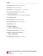
Страница 12: ...f more than 115 12 6 dB 102 4dB at the 1 23MHz band 4 3 Transmit Specification 4 3 1 Frequency Range 824 820 MHz 848 190 MHz 4 3 2 Intermediate Frequency QSC60X0 seires Zero IF 4 3 3 Output Power 0 282W 4 3 4 Interference Rejection Single Tone 30dBm at 900 kHz Two Tone 43dBm at 900 kHz 1700kHz 4 3 5 CDMA TX Frequency Deviation 300Hz or less 4 3 6 CDMA TX Conducted Spurious Emissions 900kHz 42 dBc ...

Страница 13: ...MHz 839 580 MHz 840 810 MHz 842 04 MHz 843 270 MHz 844 500 MHz 845 910 MHz 847 140 MHz 848 370 MHz 4 5 MS Mobile Station Receiver Frequency FA NO CH NO CENTER FREQUENCY FA NO CH NO CENTER FREQUENCY 1 2 3 4 5 6 7 8 9 10 1011 29 70 111 152 193 234 275 316 363 869 640 MHz 870 870 MHz 872 100 MHz 873 330 MHz 874 560 MHz 875 790 MHz 877 020 MHz 878 250 MHz 879 480 MHz 880 890 MHz 11 12 13 14 15 16 17 1...

Страница 14: ...es battery is being charged Green light indicates battry is fully charged 5 3 For Mobile Mount 5 3 1 Installation Position In order to reduce echo sound when using the Hands Free Kit make sure that the speaker and microphone are not facing each other and keep microphone a generous distance from the speaker 5 3 2 Cable Connections 5 3 2 1 Power and Ignition Cables Connect the red wire to the car ba...

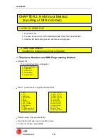
Страница 15: ...after input press OK to save To reset the handset press END CHAPTER 2 NAM Input Method Inputting of MIN included 2 NAM Input Method Inputting of telephone numbers included 1 ESN 2 MIN 3 NAM Name 4 Security Code 5 MCC 6 NMSID 7 IMSI_T MCC 8 IMSI_T NMSID 9 PRL Enabled 10 MDN 11 CDMA Home SID 12 CDMA Home NID 1 HOW TO POWER UP 13 CDMA Pri ChA 14 CDMA Sec ChA 15 CDMA Pri ChB 16 CDMA Sec ChB 17 Lockout...

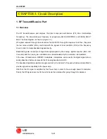
Страница 16: ...al directly Baseband signals created are changed into digital signals by the analog digital converter ADC A D Converter and then auto gain controlled and are demodulated by the modulator demodulator In the case of transmission QSC6010 modulates interpolates and converts the digital signal into an analog baseband before upconverts the Tx analog baseband into RF The baseband quadrature signals are u...

Страница 17: ...revent the drop in receive sensitivity characteristics The receive part BPF blocks the signals sent out from entering the receive end in order to improve sensitivity characteristics Insertion loss IL in the transmit band is 2 8dB Max whereas IL in the receive band is 3 5dB Max The receive band attenuation amount of transmit filter is 45dB Min and the transmit band attenuation amount of receive fil...

Страница 18: ...terpolates and converts the digital signal into an analog baseband and upconverts the Tx analog baseband into RF The QSC6010 communicates with the external RF and analog baseband to control signal gain in the RF Rx and Tx signal paths educe base band offset errors and tune the system frequency reference The QSC6010 baseband to RF Transmit Processor performs all Tx signal processing functions requi...

Страница 19: ...face circuit are integrated onto one IC after going through the GaAs HBT heterojunction bipolar transistor process The module of power amplifier is made up of an output end interface circuit including this module The maximum power that can be inputted through the input terminal is 8dBm and conversion gain is about 28 5dB RF transmit signals that have been amplified through the power amplifier are ...

Страница 20: ... operation status on to the screen and a receptacle that receives and sends out voice and data with external sources 2 2 2 Voice Processing Part The voice processing part is made up of an audio codec in QSC6010 used to convert MIC signals into digital voice signals and other external MIDI Synthesizer used to convert digital voice signals into analog voice signals amplifying parts for amplifying th...

Страница 21: ...in Table 1 2 The baseband function reduces part costs by using two external bus interfaces to support next generation memory architectures such as NAND FLASH SRAM and pseudo SRAM PSRAM page and burst mode NOR or MLC NOR FLASH The EBI2 also serves as an enhanced LCD interface A variety of connectivity options are supported the keypad interface and USB UART and RUIM ports are available A camera inte...

Страница 22: ... memory part consists of a 64Mbits Flash Memory and a 32Mbits SRAM On the Flash Memory there are programs used for the operation of a mobile station and the non volatile data of the mobile station such as a ESN Electronic Serial Number are stored The programs can be changed through down loading after the assembling of mobile stations On the SRAM data generated during the operation of a mobile stat...

Страница 23: ...us and a 32 bit internal data bus It has a high performance and low power consumption FLASH ROM and SRAM Flash Memory is used to store the program of the mobile station Using the down loading program the program can be changed even after the mobile station is fully assembled SRAM is used to store the internal flag information call processing data and timer data KEYPAD For key recognition key matri...

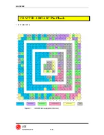
Страница 24: ...LG KD3500 LGE LG Electronics Inc 22 21 1 U201 QSC6010 CHAPTER 4 BGA IC Pin Check ...

Страница 25: ...LG KD3500 LGE LG Electronics Inc 23 21 2 U310 Memory ...

Страница 26: ...face Memory Interface Codec SPK AMP RF Interface Input Power Management General Housekeeping BB PM Block I F MIC EAR Output Voltage Reguration Connectivity UIM USB Quadrature Upconverter Quadrature Downconverter LNA RF Block BPF KD3500 Block Diagram QSC6010 SKY77162 U102 EFSD836MF1S2 DP101 TX IL 1 5 2 3 dB RX IL 2 3 3 5 dB V ref 2 85V ...

Страница 27: ...When Rx Sensitivity isn t good enough Test Point 4 1 Rx Part Trouble CHAPTER 4 Trouble Shooting CHAPTER 4 Trouble Shooting QSC6010 F101 DP101 U101 ...

Страница 28: ...Circuit Diagram DP101 DP101 ...

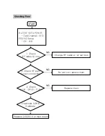
Страница 29: ...5515C Setup CH 610 1 Check RF cable Loss 2 Check RF path Circuit connection 3 Check U101 DP101 F101 Checking Flow NG Change RF cable or re set loss NG Re work or replace them NG Replace them Download S W Calibrate Replace QSC6010 or main board ...

Страница 30: ...ress H W or F7 then click offline d Click Band select to cdma Tx on Power Amp On Set channel to 610 AGC 400 Spectrum analyzer setting Oscilloscope setting 1 Check PAM Circuit 2 Check Duplexer Mobile SW Circuit 3 Check QSC6010 circuit Redownload SW CAL Duplexer PAM Mobile S W QSC6010 ...

Страница 31: ...4 2 1 Check PAM Circuit Test Point Circuit Diagram U102 Pin4 Vref 2 85V U102 Pin7 RF_OUT U102 Pin 1 8 Vcc1 2 U102 Pin2 RF_IN U102 Pin 1 8 Vcc1 2 U102 Pin4 Vref 2 85V U102 Pin2 RF_IN U102 Pin7 RF_OUT ...

Страница 32: ...xer Mobile SW Or Replace QSC6010 Check U102 Pin2 RF_IN YES Check U102 Pin4 V_ref Check F110 circuit Check Q101 circuit NO Level is 3 2V 4 2V OK YES Check U102 Pin1 8 VCC1 2 Check C203 U201 NO Output Level is Appear YES Check U102 Pin7 RF_OUT Replace U102 Waveform U102 Pin2 DCN PAM_IN U102 Pin7 DCN PAM_OUT ...

Страница 33: ...ST POINT Circuit Flow Level is Appear YES NO Level is Appear NO Replace QSC6010 Check DP101 Pin6 DUP_OUT YES Replace DP101 Replace U101 Check U101 Pin1 Duplexer DP101 Mobile S W DP101 PIN6 DP_out U101 PIN1 Mobile S W in Circuit Diagram ...

Страница 34: ...Test Points 4 3 1 Power On Trouble R217 2 6V_MSMP R244 2 65V_MSMA R224 1 2V_MSMC R404 PWR_ON_SW Circuit Diagram QSC6010 R218 2 6V_TX 4 3 Logic Part Trouble R217 R217 R244 ...

Страница 35: ...hange Battery and try again Replace U201 Re download Software Check the contact of power key or dome switch Push power on key and check the level change of R404 Check the voltage of the following port at U201 1 2V_MSMC 2 6V_MSMP 2 65V_MSMA 2 85V_TCXO 2 6V_RX 2 6V_TX ...

Страница 36: ...4 3 2 Charging Trouble Test Points Circuit Diagram CON409 CON409 pin1 ...

Страница 37: ...d NO Re solder or replace CON409 The charging adaptor TA is out of order Change the charging adaptor Voltage at Pin1 V_CHAR of CON409 5 6V YES NO YES Is the battery charged NO The battery may have the problem Change the battery and try again Charging will operate properly YES OK Check QSC6010 circuit Replace QSC6010 or mainboard NG ...

Страница 38: ...4 3 3 Audio Trouble Test Points Figure 4 3 3 RECEIVER PART Circuit Diagram U309 Pin1 QSC_AMP_OUT Pin4 COM_SPK U308 Pin1 QSC_AMP_OUT Pin4 COM_SPK Pin1 QSC_AMP_OUT Pin1 QSC_AMP_OUT Pin4 COM_SPK ...

Страница 39: ... at pin4 of U308 U309 SETTING Ringers at Sounds menu Check the connection of speaker rework or replace the speaker Re soldering or Replace the U308 U309 Replace QSC6010 or board NO Yes Yes Signal from U308 U309 pin1 Replace QSC6010 or board Speaker will work properly Yes NO ...

Страница 40: ...t points Circuit Diagram 4 3 6 MIC Trouble R326 START Signal at R326 1 8V Replace QSC6010 MIC park is OK check SPK part Checking Flow Yes NG Check MIC Re solder MIC or change MIC position is critical NG OK ...

Страница 41: ...ART D301 C324 C345 C346 Test points SETTING Vibrator on at Sounds of test menu Checking Flow START Replace QSC6010 or board No Yes Yes No Check the state of Contact of Vibrator Re contact vibrator Is the signal C346 LOW Re solder or change them Check soldering of D301 C324 C345 OK NG Change vibrator ...

Страница 42: ...4 3 8 Key Backlight LED Trouble Test Points Figure 4 3 8 KEYPAD BACK LIGHT PART Figure 4 3 8 KEYPAD Back Light Circuit LED309 LED308 LED302 LED303 LED311 LED315 LED313 LED316 VPWR Circuit Diagram ...

Страница 43: ...R319 R337 R305 R313 R316 R328 R390 R391 3 2 4 2V Check LEDs directions Charge or Change Battery and try again Check the soldering of each R or Replace them Re solder or replace LEDs NG No NG OK Yes OK Change Board Check the signal level at KYPD_EN LOW Replace QSC No ...

Страница 44: ...4 3 9 Earphone Trouble Test Points Circuit Diagram Figure 4 3 9 EAR MIC JACK PART Circuit 4 3 9 EAR MIC JACK PART CON301 R307 C307 R333 R315 L305 R308 L301 ...

Страница 45: ...y again No No Yes Yes Set the audio part of the test equipment to echo mode Earphone detect problem Audio path problem Can you hear your voice from the earphone Change Earphone Set the audio part of the test equipment to continuous wave mode Earphone receiving Path problem Can you hear the sound from the earphone Earphone sending path problem 4 2 3 Yes No Yes No Yes SETTING After initialize 5515C ...

Страница 46: ...Does it work well Re download software Does it work well 4 Change main board NG OK Yes Yes No No Earphone receiving path problem 2 Is level detected form R332 C307 L305 Check soldering of Pin 2 of CON301 Change QSC or main board Replace them or re download SW Re solder or Replace CON301 Yes Yes No ...

Страница 47: ...4 3 10 LCD Trouble Test Points Circuit Diagram C O N 3 0 4 CON304 pin3 ...

Страница 48: ...ldering or Replace R405 R477 No Does R405 R477 LCD connection Work Properly Change the Main Board Yes Check the Control signal D 0 15 LCD_RESET LCD_ID LCD_CS LCD_LIGHT Check the CON406 Soldering No Re Solder or change CON406 Change the LCD Module Yes Check LCD fpcb connection Re connect LCD fpcb NG OK ...

Страница 49: ...Checking Flow Back Light START Check the U303 pin 5 VPWR Is U303 pin3 bigger then 5V No Yes Check replace QSC Yes No Change U303 Check the signal level at LCD_BACK_EN high Replace QSC No Yes ...

Страница 50: ...CON302 Test Points Circuit Diagram 4 3 11 UIM Trouble R375 R378 R361 R376 ...

Страница 51: ...ck CON302 soldering Check UIM Card circuit R375 R378 R361 R376 START Re soldering CON302 Re solder or replace them NG NG OK OK Change main board Check if right UIM card is used Use right UIM card and try again No Yes Try after re download SW Done OK NG ...

Страница 52: ...Test Points 4 3 12 FM Radio Trouble Circuit Diagram X 1 0 1 Pin1 Q102 Pin4 R307 R332 U103 Pin8 ...

Страница 53: ...1 Freq 32 768kHz Check the condition of Q102 and external component Replace X101 Audio signal appear at R332 R307 Check the FM Receiver circuit input voltage soldering If problem replace the defected component Audio signal appear at pin6 and pin8 of U104 Check the FM AMP circuit If problem replace the defected component Refer to Earphone Trouble part Yes No Yes Yes Yes No No No ...

Страница 54: ......

Страница 55: ......

Страница 56: ......

Страница 57: ......

Страница 58: ...ubles U301 Memory Booting trouble CON302 UIM socket UIM trouble Network connection trouble CON406 35pin LCD connector LCD display trouble CON301 Ear jack connector Ear phone trouble U103 FM tuner chip FM trouble X202 X tal Power trouble No service U302 MIC connector MIC trouble CON409 Micro USB connector Power trouble Sync trouble X101 X tal FM trouble ...

Страница 59: ...ouble U201 QSC6010 All troubles U301 Memory Booting trouble CON302 UIM socket UIM trouble Network connection trouble CON406 35pin LCD connector LCD display trouble CON301 Ear jack connector Ear phone trouble X202 X tal Power trouble No service U302 MIC connector MIC trouble CON409 Micro USB connector Power trouble Sync trouble ...

Страница 60: ......

Страница 61: ...C DC 5 3 7 V 950 mAh 1 CELL PRISMATIC KU250 Europe BATT IP Pb Free 3 7 950 0 2C PRISMATIC 50x34x55 BLACK Innerpack Europe Label SBPL00 90501 BATTERY PACK LI ION 4 3 7 V 950 mAh 1 CELL PRISMATIC KU250 BATT Europe Pb Free 3 7V 950mAh 0 2C PRISMATIC 50x34x55 BLACK Innerpack Europe Label 1 SBPL00 91401 BATTERY PACK LI ION 3 PRINTING empty 1 MMBB0 267501 MANUAL OP ERATION 2 MOLD PC LUPOY HP 5004 1 MCJA...

Страница 62: ...SPFY0166502 FR 4 0 8 mm BUILD UP 4 main SPFY0166502 PCB MAIN SPFY00 352 Maker P N Specification PN Descriptio n Ref No NO ...

Страница 63: ...8810 1 CUTTING PMMA MR 200 MWAC008810 1 WINDOW LCD MWA C00 3 31 MTAD0077 301 MTAD0077301 COMPLEX empty MTAD0077301 TAPE WINDOW MTAD 00 3 30 MTAB0199 701 MTAB0199701 COMPLEX empty MTAB0199701 TAPE PROTECTION MTAB 00 3 29 MPBG0069 401 MPBG0069401 COMPLEX empty MPBG006940 1 PAD LCD MPBG 00 3 28 MFBD0027 201 MFBD0027201 COMPLEX empty MFBD0027201 FILTER MIKE MFBD 00 3 27 MFBC0035 501 MFBC0035501 COMPLE...

Страница 64: ...5101 CAN SHIELD MCBA 00 4 50 ADCA0073 301 ADCA0073301 ADCA0073301 DOME ASSY METAL ADCA 00 4 49 MLAA0002 505 ULCP_App Label MLAA0002505 LABEL APPROVAL MLAA 00 2 46 MGAZ0061 101 MGAZ0061101 CUTTING NS MGAZ0061101 GASKET MGAZ 00 2 45 GMEY0009 201 GMEY0009201 1 4 mm 3 5 mm MSWR3 BK B HEAD D 2 7mm GMEY000920 1 SCREW MACHINE BIND GMEY 00 2 44 SNMF0036 701 10LN31A7W00 0033 5 0 6 dB Internla DCN_Single Pb...

Страница 65: ...MZSJ100 R305 R313 R316 R319 R328 R337 3 6 EDLH00045 01 LG INNOTEK LED LEBB S14E LED302 LED303 LED308 LED309 LED311 LED313 2 5 100 p 100 5 1 ECZH00008 13 TDK CHIP CAPACITOR C1005C0G1H10 1JT C427 1 Toleran ce Valu e Siz e Qt y ItemNo Maker PN Desc Remark Component Name Zuken Desig No N O RD3500_MAIN_REV11_TOP ...

Страница 66: ...ECCH0000 163 TDK CHIP CAPACITOR C1005X5R473K DT C239 9 10 15n 10 05 2 ECCH0000 157 ROHM CHIP CAPACITOR MCH153CN153 KK C208 C254 8 10 10n 10 05 4 ECCH0000 155 ROHM CHIP CAPACITOR MCH153CN103 KK C124 C312 C324 R359 7 10 4 7n 10 05 1 ECCH0000 151 ROHM CHIP CAPACITOR MCH152CN472 KK C317 6 10 3 3n 10 05 1 ECCH0000 149 ROHM CHIP CAPACITOR MCH155CN332 KK C213 5 10 1n 10 05 5 ECCH0000 143 ROHM CHIP CAPACI...

Страница 67: ...OR C1005X7R1E68 2KT C308 2 2 10 8 2n 10 05 1 ECZH0001 105 TDK CHIP CAPACITOR C1005X7R1C82 2KT C246 2 1 5 33p 10 05 31 ECZH0000 830 TDK CHIP CAPACITOR C1005C0G1H33 0JT C102 C334 C335 C345 C401 C404 C 407 C408 C409 C412 C415 C417 C41 8 C421 C426 C428 C429 C430 C431 C435 C436 C437 C438 C439 C443 C 444 C446 C453 C455 R412 R418 2 0 5 12p 10 05 3 ECZH0000 816 TDK CHIP CAPACITOR C1005C0G1H12 0JT R357 R35...

Страница 68: ...6 3 5 1 6X2 7X0 8 1 EDSY0017 701 AUK SCHOTTKY SDB1040 D401 3 4 1 EDSY0009 901 KEC SWITCHING DIODE KDS160E D301 3 3 79 8 100n 1005 1 ECZH0004 402 ROHM CHIP CAPACITOR MCH153C104ZK C456 3 2 10 1u 1608 4 ECZH0003 503 MURATA CHIP CAPACITOR GRM39X5R105K25PT C302 C303 C304 C305 3 1 10 82n 1005 4 ECZH0003 125 MURATA CHIP CAPACITOR GRM36X7R823K16 C205 C247 C279 C321 3 0 10 68n 16V 1005 2 ECZH0003 124 MURAT...

Страница 69: ...1 ENSY00181 01 KSD SIM SOCKET KCN 2T 0 0075 CON302 4 8 1 ENRY0007 201 MATSUSHIT A MINI USB AXJ53314 CON409 4 7 20 4 7u 2025 1 ELCP00080 05 SAMHWA POWER INDUCTOR CPI2520LZ4R7ME L202 4 6 5 100n 1005 4 ELCH00106 28 SUNLORD CHIP INDUCTOR SDCL1005CR10JTF L106 L112 L306 L307 4 5 5 82n 1005 2 ELCH00106 27 SUNLORD CHIP INDUCTOR SDCL1005C82NJTF L109 L110 4 4 5 22n 1005 3 ELCH00106 20 SUNLORD CHIP INDUCTOR ...

Страница 70: ...F1 182 R215 6 4 1 220k 1005 1 ERHZ0000245 ROHM RESISTO R MCR01MZSF2 203 R464 6 3 1 80 6k 1005 1 ERHZ0000318 ROHM RESISTO R MCR01MZSF8 062 R223 6 2 1 470k 1005 3 ERHZ0000288 ROHM RESISTO R MCR01MZSF4 703 R214 R239 R241 6 1 1 47k 1005 1 ERHZ0000287 ROHM RESISTO R MCR01MZSF4 702 R487 6 0 1 220k 1005 1 ERHZ0000245 ROHM RESISTO R MCR01MZSF2 203 R489 5 9 1 15k 1005 1 ERHZ0000221 ROHM RESISTO R MCR01MZSF...

Страница 71: ...005 1 ERHZ0000486 ROHM RESISTOR MCR01MZSJ47 3 R225 8 1 5 4 7k 1005 1 ERHZ0000485 ROHM RESISTOR MCR01MZSJ47 2 R314 8 0 5 470 1005 8 ERHZ0000484 ROHM RESISTOR MCR01MZSJ47 1 R406 R414 R415 R421 R431 R441 R 450 R453 7 9 5 33k 1005 2 ERHZ0000466 ROHM RESISTOR MCR01MZSJ33 3 R277 R278 7 8 5 330 1005 2 ERHZ0000464 ROHM RESISTOR MCR01MZSJ33 1 L101 R106 7 7 5 22k 1005 2 ERHZ0000444 ROHM RESISTOR MCR01MZSJ22...

Страница 72: ...AD INDUCTOR BLM15HD182SN1 L305 9 8 600 1005 2 SFBH0008 101 MURATA BEAD INDUCTOR BLM15AG601SN1 L302 L303 9 7 5 6V 100p 1005 3 SEVY0003 601 INNOCHIPS VARISTOR ICVL0505101V150FR C419 R379 R437 9 6 1 SETY0004 501 MURATA THERMISTOR NCP18WM154J03RB R226 9 5 DCN 2 5X3 0X1 3 1 SDDY0004 001 EPCOS DUPLEXER B7638 DP101 9 4 2 5X3 2X0 9 1 EXXY0025 101 DAISHINKU X TAL DSX321G_19_2MHZ_8PF X202 9 3 32M_ 16 8 0X10...

Страница 73: ......
Отзывы: