LG-
K
D3500
LGE
LG Electronics Inc.
17/21
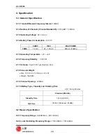
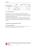
Condition Min.
Typ.
Max.
Unit
Maximum Output Power
28
dBm
Noise power
869-894 MHz, all power
levels
-135.0
dBm/Hz
ACPR
±
885kHz, < 2:1 VSWR
±
1.98MHz, < 2:1 VSWR
-44
-57
dBc
dBc
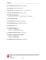
1.3.2 Power Amplifier (U102)
The power amplifier that can be used in the CDMA mode has linear amplification capability.
For higher efficiency, it is made up of one module (Monolithic Microwave Integrated Circuit) for which
RF input terminal and internal interface circuit are integrated onto one IC after going through the GaAs
HBT (heterojunction bipolar transistor) process.
The module of power amplifier is made up of an output end interface circuit including this module.
The maximum power that can be inputted through the input terminal is 8dBm and conversion gain is
about 28.5dB. RF transmit signals that have been amplified through the power amplifier are sent to
the duplexer.
1.4 Description of Frequency Synthesizer Circuit
1.4.1 Crystal Oscillator (X202)
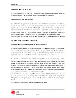
Crystal Unit generates the refrence frequency of 19.2MHz. Tolerance at 25
°
C is
±
12x10
-6
Max.Tolerance over the tmperature range is
±
12x10
-6
Max. at -30 to 85
°
C
Содержание RD3500
Страница 2: ...CDMA MOBILE SUBSCRIBER UNIT LG KD3500 SINGLE BAND CDMA MOBILE PHONE SERVICE MANUAL ...
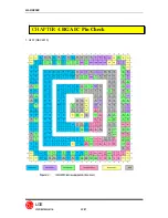
Страница 24: ...LG KD3500 LGE LG Electronics Inc 22 21 1 U201 QSC6010 CHAPTER 4 BGA IC Pin Check ...
Страница 25: ...LG KD3500 LGE LG Electronics Inc 23 21 2 U310 Memory ...
Страница 28: ...Circuit Diagram DP101 DP101 ...
Страница 36: ...4 3 2 Charging Trouble Test Points Circuit Diagram CON409 CON409 pin1 ...
Страница 47: ...4 3 10 LCD Trouble Test Points Circuit Diagram C O N 3 0 4 CON304 pin3 ...
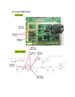
Страница 50: ...CON302 Test Points Circuit Diagram 4 3 11 UIM Trouble R375 R378 R361 R376 ...
Страница 52: ...Test Points 4 3 12 FM Radio Trouble Circuit Diagram X 1 0 1 Pin1 Q102 Pin4 R307 R332 U103 Pin8 ...
Страница 54: ......
Страница 55: ......
Страница 56: ......
Страница 57: ......
Страница 60: ......
Страница 73: ......


