LG-
K
D3500
LGE
LG Electronics Inc.
18/21
2. Digital/Voice Processing Part
2.1 Overview
The digital/voice processing part processes the user's commands and processes all the digital and
voice signal processing in order to operate in the phone. The digital/voice processing part is made up
of a keypad/LCD, receptacle part, voice processing part, mobile station modem part, memory part,
and power supply part.
2.2 Configuration
2.2.1 Keypad/LCD and Receptacle Part
This is used to transmit keypad signals to QSC6010. It is made up of a keypad backlight part that
illuminates the keypad, LCD part that displays the operation status on to the screen, and a receptacle
that receives and sends out voice and data with external sources.
2.2.2 Voice Processing Part
The voice processing part is made up of an audio codec in QSC6010 used to convert MIC signals into
digital voice signals and other external MIDI Synthesizer used to convert digital voice signals into
analog voice signals, amplifying parts for amplifying the voice signals and MIC signals are on external
MIDI Synthesizer and Codec in QSC6010.
2.2.3 QSC6010 (Mobile Station Modem) Part
QSC6010 is the core elements of a CDMA mobile station and carries out the functions of CPU,
encoder, interleaver, deinterleaver, Viterbi decoder, Mod/Demod, codec, and vocoder.with RF, and PA
module
2.2.4 Memory Part
The memory part is made up of a flash memory, SRAM for storing data.
Содержание RD3500
Страница 2: ...CDMA MOBILE SUBSCRIBER UNIT LG KD3500 SINGLE BAND CDMA MOBILE PHONE SERVICE MANUAL ...
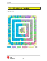
Страница 24: ...LG KD3500 LGE LG Electronics Inc 22 21 1 U201 QSC6010 CHAPTER 4 BGA IC Pin Check ...
Страница 25: ...LG KD3500 LGE LG Electronics Inc 23 21 2 U310 Memory ...
Страница 28: ...Circuit Diagram DP101 DP101 ...
Страница 36: ...4 3 2 Charging Trouble Test Points Circuit Diagram CON409 CON409 pin1 ...
Страница 47: ...4 3 10 LCD Trouble Test Points Circuit Diagram C O N 3 0 4 CON304 pin3 ...
Страница 50: ...CON302 Test Points Circuit Diagram 4 3 11 UIM Trouble R375 R378 R361 R376 ...
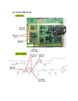
Страница 52: ...Test Points 4 3 12 FM Radio Trouble Circuit Diagram X 1 0 1 Pin1 Q102 Pin4 R307 R332 U103 Pin8 ...
Страница 54: ......
Страница 55: ......
Страница 56: ......
Страница 57: ......
Страница 60: ......
Страница 73: ......


