LG-
K
D3500
LGE
LG Electronics Inc.
21/21
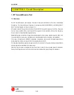
2.3.5 Logic Part
The Logic part consists of internal CPU of QSC6010, MCP (SRAM+FLASH ROOM).
The QSC6010 receives X-tal(19.20MHz) clock signals, and then controls the phone during the CDMA
mode. The major components are as follows:
CPU : ARM926EJ-S microprocessor core
MEMORY :
•
FLASH ROM : 64Mbits (U301, PF38F2040W0YBQ0)
•
STATIC RAM : 32Mbits (U301, PF38F2040W0YBQ0)
CPU
The ARM7TDMI 32-bit microprocessor is used and CPU controls all the circuitry. Some of the
features of the ARM microprocessor include a 3 stage pipelined RISC architecture, both 32-bit ARM
and 16-bit THUMB instruction sets, a 32-bit address bus, and a 32-bit internal data bus. It has a high
performance and low power consumption.
FLASH ROM and SRAM
Flash Memory is used to store the program of the mobile station. Using the down-loading program,
the program can be changed even after the mobile station is fully assembled.
SRAM is used to store the internal flag information, call processing data, and timer data.
KEYPAD
For key recognition, key matrix is setup using KEY_SENSE[0]-[4] signals and GPIO of output ports
of QSC6010. 8 LEDs and backlight circuitry are included in the keypad for easy operation in the
dark.
LCD MODULE
LCD module contains a controller which will display the information onto the LCD by 16-bit data
from the QSC6010. It is also supplied stable 1.8V_MSM_E1 by inner regulator in U201 for fine view
angle and and LCD reflects to improve the display efficiency.
Содержание RD3500
Страница 2: ...CDMA MOBILE SUBSCRIBER UNIT LG KD3500 SINGLE BAND CDMA MOBILE PHONE SERVICE MANUAL ...
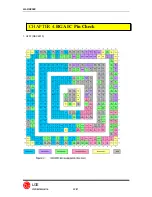
Страница 24: ...LG KD3500 LGE LG Electronics Inc 22 21 1 U201 QSC6010 CHAPTER 4 BGA IC Pin Check ...
Страница 25: ...LG KD3500 LGE LG Electronics Inc 23 21 2 U310 Memory ...
Страница 28: ...Circuit Diagram DP101 DP101 ...
Страница 36: ...4 3 2 Charging Trouble Test Points Circuit Diagram CON409 CON409 pin1 ...
Страница 47: ...4 3 10 LCD Trouble Test Points Circuit Diagram C O N 3 0 4 CON304 pin3 ...
Страница 50: ...CON302 Test Points Circuit Diagram 4 3 11 UIM Trouble R375 R378 R361 R376 ...
Страница 52: ...Test Points 4 3 12 FM Radio Trouble Circuit Diagram X 1 0 1 Pin1 Q102 Pin4 R307 R332 U103 Pin8 ...
Страница 54: ......
Страница 55: ......
Страница 56: ......
Страница 57: ......
Страница 60: ......
Страница 73: ......


