BT900-Sx Hardware Integration Guide
Intelligent BTv4.0 Dual Mode Module
Embedded Wireless Solutions Support Center:
http://ews-support.lairdtech.com
www.lairdtech.com/bluetooth
15
Americas: +1-800-492-2320
Europe: +44-1628-858-940
Hong Kong: +852 2923 0610
seconds; start-up time is the time taken from power-up to being able to run a smart BASIC
command. Most of this is for radio initialisation. 1.6 seconds is also the time when coming out
of reset through AT command (atz) or AT command for factory default (at&f*).
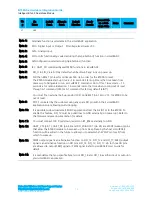
Note 4:
The Bluetooth chip in the BT900 has two internal regulators, a high voltage (input pin
BT_VREG_IN_HV) and low voltage (input pin BT_VREG_OUT_HV) regulator. ONLY ONE
regulator MUST be used to power the radio chip.
Method 1: If the BT900 is required to operate from 3.3V, connect the external 3.3V
supply to pin 31 (BT_VREG_IN_HV), pin 5 (VCC), and pin 43 (BT_VDD_IO). Customer
MUST leave pin 32 (BT_VREG_OUT_HV) unconnected.
Method 2: If the BT900 is required to operate from 1.8V, connect the external 1.8V
supply to pin 32 (BT_VREG_OUT_HV), pin 5 (VCC) and pin 43 (BT_VDD_IO). Customer
MUST leave pin 31 (BT_VREG_IN_HV) unconnected.
Note that 1.8V operation is not supported in current
smart
BASIC runtime engine FW v9.1.2.0.
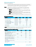
Table 5: Signal Levels for Interface, SIO
Parameter
Condition
Min
Typ
Max
Unit
VIH Input high voltage
VCC < 2.7V
VCC
≥
2.7V
0.7VxCC
0.8VxCC
VCC+0.3
VCC+0.3
V
VIL Input low voltage
VCC < 2.7V
VCC
≥
2.7V
VSS-0.3
0.3xVCC
0.2xVCC
V
V
VOH Output high voltage
(std. drive, 4mA) See
VCC < 2.7V
VCC
≥
2.7V
VCC-0.45
VCC-0.5
VCC
VCC
V
V
VOL Output low voltage
(std. drive, 4mA)
VCC < 2.7V
VCC
≥
2.7V
VSS
VSS
0.4
0.4
V
V
Pull up resistance
VCC < 2.7V
VCC
≥
2.7V
-
21
-
33
134
66
k
Ω
k
Ω
Input capacitance
5
15
pF
Note 1: 50mA is the total average SIO pin output current which is defined as the average current value
flowing through all of the corresponding pins for a 100mS period.
Table 6: SIO pin alternative function AIN (ADC) specification
Parameter
Min
Typ
Max
Unit
AVCC (AVCC = VCC)
1.75
3.3
3.6
V
AVCC current draw (ADC 1 unit operation)
0.27
0.42
mA
AVCC current draw (ADC stop)
0.03
10
uA
AVREF (when AVCC
≥
2.7V 2.7 V
AVCC
V
AVREF (when AVCC < 2.7V)
AVCC
AVCC
V
AVREF current draw (ADC 1 unit operation)
0.72
1.29
mA
AVREF current draw (ADC stop)
0.02
2.6
uA
ADC input pin (AIN) voltage maximum
VSS
AVREF
V
ADC input port (AIN) current draw
5
uA
Time required to convert single sample
12 bit mode
2
10
uS
ADC input resistor impedance (during
operation) (
AVCC
≥
2.7V
2.2
kOhm

