background image

BT900-Sx Hardware Integration Guide 

Intelligent BTv4.0 Dual Mode Module 

Embedded Wireless Solutions Support Center: 
http://ews-support.lairdtech.com


www.lairdtech.com/bluetooth


28


Americas: +1-800-492-2320 

Europe: +44-1628-858-940 

Hong Kong: +852 2923 0610


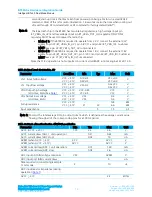
SIO pin direction 
For BT900 modules shipped from production with 

smart


BASIC runtime engine firmware, most SIO pins 

(with a default function of DIO) are digital inputs (see 

Table 2

). Remember to change the direction SIO 

pin (in your 

smart


BASIC application script) if that particular pin is wired to a device that expects to be 

driven by the BT900 SIO pin configured as an output. Also, SIO pins that are inputs are set in firmware 
by default to have internal pull-up resistor enabled (on SIO_xx pins, not BT_xxxx pins). You may 
configure this in your 

smart

BASIC application script.   

Note:     The internal pull-up takes current from VCC. 

Lowest power consumption is achieved when all SIO pins are set as outputs and low.             


SIO_19 pin and VSP Command       

        SIO_19 pin must be pulled to GND externally to enable VSP (virtual serial Port) Command mode for 

BLE. SIO_19 is an input, set with internal pull-up in the firmware. VSP Command mode is used to load 
smartBASIC scripts OTA (over the air) from a BLE-enabled host.   


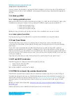
nRESET pin (active low) 
Hardware reset. Wire out to push button or drive by host.   
By default, the module is out of reset (internal weak-pull-up) when power is applied to the VCC pin.     
You MUST fit an external pull-up resistor (10K) on nRESET (pin 16) to VCC for the BT900 to be out of 
reset. nRESET needs to be held low (0V)for greater than 500nS to reset the module.     

6.2


PCB Layout on Host PCB - General     

PCB Checklist 


You 

MUST

 place the BT900-Sx module close to the edge of PCB (mandatory for BT900-SA for on-board 

chips antenna to radiate properly). 


Use solid GND plane on the inner layer (for best EMC and RF performance). 


All module GND pins MUST be connected to host PCB GND. 


Place GND vias as close to module GND pads as possible. 


Unused PCB area on surface layer can be flooded with copper but place GND vias regularly to connect 
copper flood to inner GND plane. If GND, flood copper underside the module then connect with GND 
vias to inner GND plane. 


Route traces to avoid noise being picked up on VCC supply and AIN (analogue) and SIO (digital) traces. 


Do 

NOT

 run any track near pin 34 of the BT900-Sx.   


Ensure no exposed copper is on the underside of the module (refer to land pattern of BT900 
development board).       

6.3


PCB Layout on Host PCB for BT900-SA     

6.3.1


Antenna keep-out on host PCB   

The BT900-SA has an integrated chip antenna and its performance is sensitive to host PCB. It is critical to 
locate the BT900-SA on the edge of the host PCB (or corner) to allow the antenna to radiate properly. Refer 
to guidelines in section 

Host PCB Land Pattern and Antenna Keep-out for BT900-SA

Some of those 

guidelines are repeated below.     


Ensure there is no copper in the antenna keep-out area on any layers of the host PCB. Keep all 
mounting hardware and metal clear of the area to allow proper antenna radiation. 


For best antenna performance, place the BT900-SA module on the edge of the host PCB, preferably in 
the corner with the antenna facing the corner. 


The BT900 development board has the BT900-SA module on the edge of the board (not in the corner).     
The antenna keep-out area is defined by the BT900 development board which was used for module 
development and antenna performance evaluation is shown in 

Figure 4

, where the antenna keep-out 

Содержание BT900-SA-0x

Страница 1: ...art BT900 SA 0x BT900 SC 0x HARDWARE INTEGRATION GUIDE VERSION 1 6 Americas 1 800 492 2320 Europe 44 1628 858 940 Hong Kong 852 2923 0610 Embedded Wireless Solutions Support Center http ews support lairdtech com www lairdtech com bluetooth ...

Страница 2: ...ge History Approved By 1 0 Initial Version Jonathan Kaye 1 1 13 Feb 2015 Added system clock and tick count period table Jonathan Kaye 1 2 24 Feb 2015 Edits to clarify OTA app download works over VSP command mode Jonathan Kaye 1 3 01 July 2015 Updated SPP range to reflect Up to 600 kpbs Ben Whitten 1 4 21 July 2015 Added Tape and Reel information Maggie Teng 1 5 15 Oct 2015 Updated SIG Qualificatio...

Страница 3: ...ameters 14 3 3 3 nAutoRUN pin and Operating Modes 17 3 3 4 OTA Over the Air smart BASIC application download 17 4 Power Consumption 18 4 1 Power Consumption across Clock Frequencies 18 5 Functional Description 20 5 1 Power Management includes brown out and power on reset 20 5 2 Clocks and Timers 21 5 2 1 Clocks 21 5 2 2 Timers 21 5 3 Memory for smart BASIC Application Code and Data 21 5 4 RF 21 5 ...

Страница 4: ...mity to Metal or Plastic 29 6 4 External Antenna Integration with BT900 SC 29 7 Mechanical Details 30 7 1 BT900 Mechanical Details 30 7 2 Host PCB Land Pattern and Antenna Keep out for BT900 SA 31 8 Application Note for Surface Mount Modules 32 8 1 Introduction 32 8 2 Shipping 32 8 2 1 Tray Package 32 8 2 2 Tape and Reel Package Information 33 8 3 Reflow Parameters 36 9 FCC and IC Regulatory State...

Страница 5: ...ries This allows developers the flexibility of utilising the Core and BLE specific smartBASIC functions from the BL6xx series to create fully interchangeable BLE applications between these product ranges Without the need for any external processor a simple smartBASIC application encapsulates the complete end to end process of reading writing and processing of sensor data and then using Classic Blu...

Страница 6: ...ytes GPIO 18 maximum configurable lines O P drive strength 4 mA Pull up resistor 33 KOhms control via smartBASIC Read pin level I2C Interface 1 configurable from GPIO total Up to 400 kbps SPI 1 configurable from GPIO total Up to 4 Mbps ADC Interface 2 channels configured from GPIO total Up to 12 bit resolution Conversion time 2 0uS at VCC 2 7V to 3 6V Reference voltage AVCC external same as VCC pr...

Страница 7: ... signal wakeup See Note 5 User Configurable Clocking User configurable clocking 40MHz 20MHz 4MHz so user can reduce current consumption further Physical Dimensions 19 mm x 12 5 mm x 2 5 mm Pad Pitch 0 8 mm Environmental Operating 40 C to 85 C Storage 40 C to 85 C Miscellaneous Lead Free Lead free and RoHS compliant Warranty One Year Development Tools Development Kit Development board and free soft...

Страница 8: ... low in your smartBASIC application script In deep sleep 7uA can be achieved if all SIO pins are set as output and low Note 6 1 8V operation not supported in current smartBASIC runtime engine FW v9 3 HARDWARE SPECIFICATIONS 3 1 Block Diagram and Pin out smartBASIC run time engine provides safe access to BT BLE stack drivers and non vol stores Non Vol File System for smartBASIC Apps Non Vol Data St...

Страница 9: ...Pin Name Default Funct Alternate Funct Default Direction Supply Domain Internal Pull up or Pull down State Notes Comment 1 UART_CTS UART SIO_3 or WKUP4 or Ext Interrupt IN VCC Pull up 1 2 6 7 12 2 SIO_4 DIO IN VCC Pull up 2 Laird Devkit UART_DTR via CON12 3 nAutoRUN SIO_22 or Ext Interrupt IN VCC Pull up In ONLY 1 2 12 Laird Devkit UART_DSR via CON12 4 SIO_5 DIO Ext Interrupt IN VCC Pull Up 1 2 12...

Страница 10: ...SIO_10 DIO I2C SDA IN VCC Pull Up 1 2 6 I2COPEN in smartBASIC selects I2C function 12 SIO_11 DIO I2C SCL IN VCC Pull Up 1 2 6 13 GND 14 SIO_12 DIO FREQ or PWM IN VCC Pull Up 1 2 13 Laird Devkit Buzzer output via CON15 15 SIO_13 DIO FREQ or PWM IN VCC Pull Up 1 2 13 Laird Devkit Button1 input 16 nRESET IN VCC Pull Up 8 System Reset Active low 17 SIO_14 DIO IN VCC N A 2 14 18 SIO_15 DIO IN VCC Pull ...

Страница 11: ... 33 GND DIO 34 BT_Ext_DS_CLK DIO IN BT_VDD_IO Weak Pull down Do not connect 35 BT_NC DIO OUT BT_VDD_IO Weak Pull down Do not connect 36 BT_NC DIO OUT BT_VDD_IO Weak Pull down Do not connect 37 BT_NC OUT BT_VDD_IO Weak Pull down Do not connect 38 BT_NC NC IN BT_VDD_IO Weak Pull down Do not connect 39 BT_ACTIVE DIO OUT BT_VDD_IO Weak Pull down 17 Do not connect 40 WLAN_ACTIVE DIO INs BT_VDD_IO Weak ...

Страница 12: ...onds is also the time when coming out of reset through AT command ATZ or AT command for factory default at f You must fit an external pull up resistor 10K on nRESET pin 16 to VCC for BT900 to be out of reset Note 9 SPI CS is created by the customer using any spare SIO pin within their smartBASIC application script allowing multi dropping Note 10 It is possible to download smart BASIC applications ...

Страница 13: ...BASIC runtime engine FW loaded but no onboard smartBASIC application script Because of this it starts up in AT command mode by default At reset all SIO lines are configured as the defaults shown above SIO lines can be configured through the smart BASIC application script to be either inputs with pull ups or none or outputs When an alternative SIO function is selected such as I2C or SPI the firmwar...

Страница 14: ...m output current 100 mA SIO H level total maximum output current 100 mA Storage temperature 40 85 ºC 3 3 2 Recommended Operating Parameters Table 4 Power Supply Operating Parameters Parameter Min Typ Max Unit VCC Note 1 Note4 1 75 3 3 3 6 V AVCC AVCC VCC Note 1 1 75 3 3 3 6 V AVREF1 when AVCC 2 7V AVREF1 when AVCC 2 7V 2 7V AVCC AVCC AVCC V VCC Maximum ripple or noise Note 2 10 of VCC VCC rise tim...

Страница 15: ... Note that 1 8V operation is not supported in current smartBASIC runtime engine FW v9 1 2 0 Table 5 Signal Levels for Interface SIO Parameter Condition Min Typ Max Unit VIH Input high voltage VCC 2 7V VCC 2 7V 0 7VxCC 0 8VxCC VCC 0 3 VCC 0 3 V VIL Input low voltage VCC 2 7V VCC 2 7V VSS 0 3 0 3xVCC 0 2xVCC V V VOH Output high voltage std drive 4mA See Note 1 VCC 2 7V VCC 2 7V VCC 0 45 VCC 0 5 VCC ...

Страница 16: ...mpedance is 2 2 10 5k Figure 3 ADC Diagram Rext Output impedance of external circuit kOhms Rext Sampling time nS Ts RAIN Rext x CAIN x 9 RAIN Input resistor of ADC kOhms 2 2kOhms at 2 7V AVCC 3 6V Input resistor of ADC kOhms 5 5kOhms at 1 8V AVCC 2 7V CAIN Input capacity of ADC pF 9 4pF at 8V AVCC 3 6V You MUST fit an external series resistor Rext when using ADC pins whose value is selected to get...

Страница 17: ... line nAutoRUN pin needs to be externally held high or low to select between the two BT900 operating modes Self contained Run mode nAutoRUN pin held at 0V Interactive Development mode nAutoRUN pin held at VCC The smartBASIC runtime engine firmware checks for the status of nAutoRUN during power up or reset If it is low and if there is a smartBASIC application named autorun then the smartBASIC runti...

Страница 18: ...nt TX pwr 8 dBm 85 85 85 mA TX only run peak current TX pwr 4 dBm 71 71 71 mA TX only run peak current TX pwr 0 dBm 61 61 61 mA TX only run peak current TX pwr 4 dBm 55 55 55 mA TX only run peak current TX pwr 8 dBm 52 52 52 mA TX only run peak current TX pwr 12 dBm 49 49 49 mA TX only run peak current TX pwr 16 dBm 48 48 48 mA TX only run peak current TX pwr 20 dBm 48 48 48 mA RX only peak curren...

Страница 19: ...consumption set all SIO pins as outputs and set low In Deep Sleep everything is disabled and the only wake up sources are reset and changed on pins on which sense is enabled The current typical consumption is 233 uA 7uA may be achieved if all SIO pins are set to outputs and low Current smartBASIC runtime engine firmware v9 1 2 0 requires a hardware reset to come out of deep sleep Future firmware r...

Страница 20: ...e 6 At 4 MHz clocking slower throughput 5 FUNCTIONAL DESCRIPTION The BT900 dual mode BT BLE module is a self contained Bluetooth Low Energy product and requires only power and a user s smartBASIC application to implement full BLE functionality The integrated high performance antenna combined with the RF and base band circuitry provides the Bluetooth Low Energy wireless link and any of the SIO line...

Страница 21: ... resolution of the regular timer is dependent on the selected system clock frequency can be obtained from Table 10 Table 10 System Clock and Tick Count Period System Clock MHz Tick Count Period uS 40 6 4 20 12 8 4 64 Tick Timer This is a 31 bit free running counter that increments every one millisecond The resolution of this counter is dependent on the selected system clock frequency and can be ob...

Страница 22: ...ng the following signals Port TXD of the application sends data to the module s UART_RX signal line Port RXD of the application receives data from the module s UART_TX signal line Note The BT900 serial module output is at 3 3V CMOS logic levels tracks VCC Level conversion must be added to interface with an RS 232 level compliant interface Some serial implementations link CTS and RTS to remove the ...

Страница 23: ...5 7 I2C Interface The I2C interface is an alternate function on SIO pins configurable by smartBASIC command The two wire interface can interface a bi directional wired OR bus with two lines SCL SDA and has master slave topology The interface is capable of clock stretching Data rates of 100 kbps and 400 kbps are supported An I2C interface allows multiple masters and slaves to communicate over a sha...

Страница 24: ...lected using the GpioSetFunc function PWM output signal has a frequency and duty cycle property PWM output is generated using 32 bit hardware timers The timers are clocked by a 4 MHz clock source Frequency is adjustable up to 1 MHz and the Duty cycle can be set over range from 0 to 100 both configurable by smartBASIC command Note The frequency driving the two SIO pins is the same but the duty cycl...

Страница 25: ...ff in Run and Standby Doze modes The module is placed automatically in Standby Doze if there are no events pending when waitevent statement is encountered within a customer s smartBASIC script The module will wake up from Standby Doze via an interrupt e g received character on the UART Rx line The module wakes up every millisecond to service the interrupt If the module receives a UART character fr...

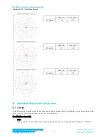
Страница 26: ... Peak gain Avg gain XY plane 2 6 7 4 Peak gain Avg gain XZ plane 2 8 5 9 Peak gain Avg gain YZ plane 1 6 4 7 6 HARDWARE INTEGRATION SUGGESTIONS 6 1 Circuit The BT900 series module is easy to integrate and requires few external components on your board aside from what is required for development and in the end application Checklist for schematic VCC External power source within the operating range ...

Страница 27: ...If not using the ADC convertor connect AVCC VCC You must connect a 100 K pull down resistor on BT_ SEL externally to GND AIN ADC and SIO pin IO voltage levels BT900 SIO voltage levels are at VCC Ensure that input voltage levels into SIO pins are also at VCC if VCC source is a battery whose voltage will drop Ensure that the ADC pin maximum input voltage for damage is not violated Filter the externa...

Страница 28: ...l PCB Checklist You MUST place the BT900 Sx module close to the edge of PCB mandatory for BT900 SA for on board chips antenna to radiate properly Use solid GND plane on the inner layer for best EMC and RF performance All module GND pins MUST be connected to host PCB GND Place GND vias as close to module GND pads as possible Unused PCB area on surface layer can be flooded with copper but place GND ...

Страница 29: ...tom and 30 mm left or right Metal in close proximity to the BT900 SA chip monopole antenna bottom top left right any direction will have degradation on the antenna performance The amount of degradation is system dependent some testing will be required in your host application The presence of metal closer than 20 mm starts to significantly degrade performance S11 gain radiation efficiency We recomm...

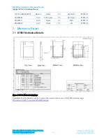
Страница 30: ...ng Kong 852 2923 0610 S181FL L RMM 2450S Nearson Dipole 2 0 uFL Note 1 BT900 SC MAF94045 Laird PCB Dipole 2 0 uFL Note 1 BT900 SC MAF94017 Laird Dipole 2 0 SMA BT900 SC MAF94019 Laird Dipole 1 5 uFL BT900 SC 7 MECHANICAL DETAILS 7 1 BT900 Mechanical Details Figure 5 BT900 Mechanical drawings Development Kit Schematics can be found in the documentation tab of the BT900 product page http www lairdte...

Страница 31: ...For BT900 SA has on board chip antenna best antenna performance the module BT900 SA MUST be placed on the edge of the host PCB and preferably in the corner with the antenna facing the corner Above Keep Out Area is the module placed in corner of PCB If BT900 SA is not placed in corner but on edge of host PCB the antenna Keep Out Area is extended see Note4 4 BT900 development board has BT900 SA plac...

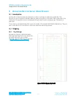
Страница 32: ... provide additional guidance beyond the information that is presented in the User Guide This application note is considered a living document and is updated as new information is presented The modules are designed to meet the needs of a number of commercial and industrial applications They are easy to manufacture and conform to current automated manufacturing processes 8 2 Shipping 8 2 1 Tray Pack...

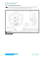
Страница 33: ...h com www lairdtech com bluetooth 33 Americas 1 800 492 2320 Europe 44 1628 858 940 Hong Kong 852 2923 0610 8 2 2 Tape and Reel Package Information Note Ordering information for Tape and Reel packaging is an addition of T R to the end of the full module part number For example BT900 SC 0x becomes BT900 SC 0x T R Figure 8 Reel specifications ...

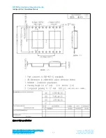
Страница 34: ...ntelligent BTv4 0 Dual Mode Module Embedded Wireless Solutions Support Center http ews support lairdtech com www lairdtech com bluetooth 34 Americas 1 800 492 2320 Europe 44 1628 858 940 Hong Kong 852 2923 0610 Figure 9 Tape specifications ...

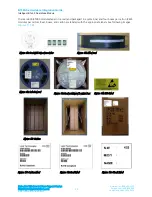
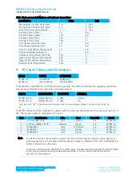
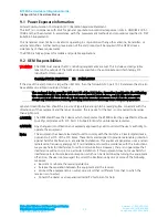
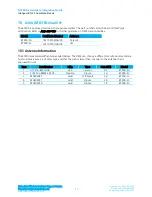
Страница 35: ... 0610 There are 600 BT900 modules taped in a reel and packaged in a pizza box and four boxes per carton 2400 modules per carton Reel boxes and carton are labeled with the appropriate labels See following images Figures 11 18 Figure 10 Reel with taped modules Figure 11 Filled reel Figure 12 Labeled reel Figure 13 Reel packaged in pizza box Figure 14 ESD label Figure 16 Carton Figure 17 Carton label...

Страница 36: ...ot manufactured before exceeding their floor life should be re packaged with fresh desiccate and a new humidity indicator card Floor life for MSL Moisture Sensitivity Level 3 devices is 168 hours in ambient environment 30 C 60 RH Table 17 Recommended baking times and temperatures MSL 125 C Baking Temp 90 C 5 RH Baking Temp 40 C 5 RH Baking Temp Saturated 30 C 85 Floor Life Limit 72 hours 30 C 60 S...

Страница 37: ...ld full modular approvals The OEM must follow the regulatory guidelines and warnings listed below to inherit the modular approval PART FORM FACTOR TX OUTPUT ANTENNA BT900 SA 0X Surface Mount 8 dBm Ceramic BT900 SC 0X Surface Mount 8 dBm u FL Last two slots 0X in Part are used for production firmware release changes Can be values 01 99 aa zz The BT900 family has been designed to operate with the an...

Страница 38: ... must accept any interference received including interference that may cause undesired operation Label and text information should be in a size of type large enough to be readily legible consistent with the dimensions of the equipment and the label However the type size for the text is not required to be larger than eight point CAUTION The OEM should have their device which incorporates the BT900 ...

Страница 39: ... exposition aux radiations Ce EUT est conforme avec SAR pour la population générale limites d exposition non contrôlée à IC RSS 102 et a été testé en conformité avec les méthodes de mesure et procédures spécifiées dans la norme IEEE 1528 Modular Approval OEM integrator is still responsible for testing their end product for any additional compliance requirements required with this module installed ...

Страница 40: ...idance on OEM s responsibilities Model Certificate Number Antenna BT900 SA 142150156 AA 00 Ceramic BT900 SC 142150157 AA 00 uFL 10 1 Antenna Information The BT900 was tested with antennas listed below The OEM can choose a different manufacturers antenna but must make sure it is of same type and that the gain is lesser than or equal to the antenna that is approved for use Item Part Number Mfg Type ...

Страница 41: ...ir device into an EU member country to make sure all regulatory requirements have been met for their complete device Table 19 provides a full list of the standards to which the modules were tested Test reports are available from the website s product page 11 1 Antenna Information The antennas listed below were tested for use with the BT900 For CE mark countries the OEM is free to use any manufactu...

Страница 42: ...ect to electromagnetic compatibility EN 301 489 1 V1 9 2 2011 09 EN 301 489 17 V2 2 1 2012 09 Emissions EN55022 2006 A1 2007 Class B Immunity EN61000 4 2 2009 EN61000 4 3 2006 A1 2008 A2 2010 3 2 Means of the efficient use of the radio frequency spectrum EN 300 328 V1 8 1 2012 06 Declaration We Laird declare under our sole responsibility that the essential radio test suites have been carried out a...

Страница 43: ...ebsite BT900 Laird Technologies D023116 58778 https www bluetooth org tpg QLI_viewQDL cfm qid 23116 Bluetopia Host StoneStreet One B019355 37180 https www bluetooth org tpg QLI_viewQDL cfm qid 19355 BlueTopia Profile StoneStreet One B020402 42849 https www bluetooth org tpg QLI_viewQDL cfm qid 20402 It is a mandatory requirement of the Bluetooth Special Interest Group SIG that every product implem...

Страница 44: ...reet One Bluetopia Profile Subsystem Select your pre paid Declaration ID from the drop down menu or go to the Purchase Declaration ID page Note Unless the Declaration ID is pre paid or purchased with a credit card you cannot proceed until the SIG invoice is paid Once all the relevant sections of step 1 are finished complete steps 2 3 and 4 as described in the help document accessible from the site...

Страница 45: ... to notify any person or entity of such revision Copying duplicating selling or otherwise distributing any part of this product or accompanying documentation software without the prior consent of an authorized representative of Laird Technologies Inc is strictly prohibited All brands and product names in this publication are registered trademarks or trademarks of their respective holders This mate...

Отзывы: