BT900-Sx Hardware Integration Guide
Intelligent BTv4.0 Dual Mode Module
Embedded Wireless Solutions Support Center:
http://ews-support.lairdtech.com
www.lairdtech.com/bluetooth
16
Americas: +1-800-492-2320
Europe: +44-1628-858-940
Hong Kong: +852 2923 0610
Parameter
Min
Typ
Max
Unit
1.8V
≥
AVCC < 2.7V
5.5-10.5
kOhm
ADC input capacitance impedance
(during operation)
1
9.4
pF
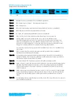
Note 1: ADC input impedance is estimated mean impedance of the ADC (AIN) pins. The ADC is highly
sensitive to the impedance of the source. The ADC (AIN) input impedance is 2.2-10.5k. Normally,
when not sampling, the ADC (AIN) impedance will have very high value and can be considered an
open circuit. The moment ADC is sampling, ADC(AIN) impedance is 2.2-10.5k.
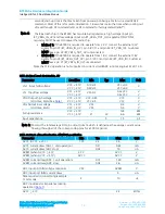
Figure 3: ADC Diagram
R
ext
: Output impedance of external circuit (kOhms)
R
ext
: Sampling time (nS)
T
s
≥
(R
AIN
+ R
ext
) x C
AIN
x 9
R
AIN
: Input resistor of ADC(kOhms)=2.2kOhms at 2.7V
≤
AVCC
≤
3.6V
Input resistor of ADC(kOhms)=5.5kOhms at 1.8V
≤
AVCC
≤
2.7V
C
AIN
: Input capacity of ADC(pF)=9.4pF at .8V
≤
AVCC
≤
3.6V
You MUST fit an external series resistor (R
ext
) when using ADC pins, whose value is selected to get required
Sample Time (T
s
). 1K to 10K may be suitable.
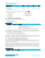
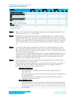
Table 7: Digital I/O Characteristics (ONLY those BT900 IO pins with names beginning with “BT_”)
Normal Operation
Min
Typ
Max
Unit
Input Voltage
VIL input logic level low
-0.4
-
0.4
V
VIH input logic level high
0.7 x BT_VDD_IO
-
BT 0.4
V
Output Voltage
VOL output logic level low, IOL = 4.0 mA
-
-
0.4
V
VOH output logic level high, IOL = 4.0 mA
0.75 x
BT_VDD_IO
-
-
V
Input and Tristate Currents
Strong pull-up
-150
-40
-10
µA
Strong pull-down
10
40
150
µA

