


1
1
2
2
3
3
4
4
D
D
C
C
B
B
A
A
Title
Number
Revision
Size
A4
Date:
2007-7-26
Sheet of
File:
X:\PT6500\.. \PLL.SchDoc
Drawn By:
PLL-LE
PLL-CLK
PLL-DA
PLL-UL
PLL IC
IC2
QT TCXO
5C
LOOP FILTER
RIPPLE
FILTER
VCO
Q6
BUFF
Q5
Q4
RF AMP
5C
Q14
ADF4111
MOD
12.8MHz
X1
TCXO
5C
TX
VCO
Q11
RX
Q8
BUFF
5C
1
1
2
2
3
3
4
4
D
D
C
C
B
B
A
A
Title
Number
Revisio n
Size
A4
Date:
2007-7-26
Sheet of
File:
X:\PT6500
\..\Receive
r.SchDoc
Drawn By:
MCF
51.65MHz
IF SY STEM
CF1
450KHz H
CF2
450KHz F
X3 mu
ltiply
AF AMP
TCXO
12.8MHz
AK2346
BPF
RF AMP
BPF
ANT SW
ANT
IC7
MCU
1st Local OSC
D1 D39 D7 D8
Q18
Q19
IC4
IC6
IC9 TDA8541
3
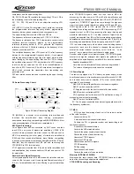
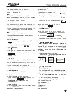
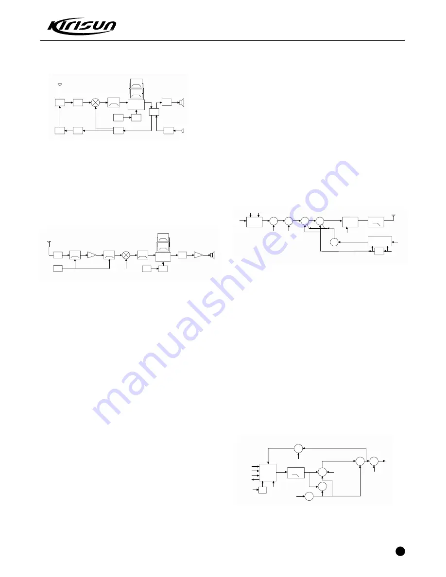
The receiver's first local oscillation is generated by the frequency
synthesizer. The second local oscillation adopts the 4th harmonic
51.2MHZ of TCXO.
The transmitter signals are generated by frequency synthesizer.
The reference frequency of frequency synthesizer is generated by
TCXO.
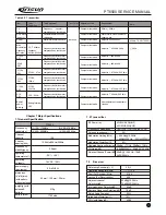
3.2 Receiver (RX) Illustration
Figure 3.2 Receiver Illustration
The Receiver Front Terminal
Signals from the antenna pass through the RX/TX switch (D1, D39,
D7, D8); and then undesirable out-of-band signals will be filtered
out at the band pass filter (BPF) consisting of two-stage LC; then
signals are amplified at the low noise amplifier (LNA) consisting of
Q18 and its peripheral components.
The output from the LNA passes the BPF consisting of three-stage
LC for filtering and then is sent to the first grade frequency mixer
(Q19).
AGC Circuit
The AGC circuit consists of Q17 and its peripheral components.
Only when the input signal is too large can the AGC functions to
reduce the Q18 plus.
The First Frequency Mixer
After mixing the receiving signals for LNA and the first local
st
oscillation signals from the frequency synthesizer, the 1 IF signals
(51.65MHz) are generated.
IF Circuit
st
Signals of adjacent channel and those out of band of the 1 IF
signals are filtered via the crystal filter (XF1).
st
The 1 IF signals from the crystal filter are amplified at the first
IF amplifier (Q20), and then are sent to the IF processing IC
(IC4, TA31136).
nd
nd
The IF IC consists of the 2 frequency mixer, the 2 local oscillator,
IF amplifier, limiter, phase frequency detector, and noise amplifier.
nd
The 2 local oscillation is obtained after 12.8MHz signals from X1
are amplified via Q15 and external circuit. The 2nd local oscillation
st
(51.2 MHz) and the 1 IF signal (51.65 MHz) are mixed at IC5 to
generate the 2nd IF (450 kHz). After the 2nd IF signal is amplified
and its amplitude is limited at IC4, and then filtered at porcelain filter
(CF1 or CF2, 450 kHz), IC5 demodulates and sends out audio
signals.
nd
The 2 IF filter selector circuit consists of CF1, CF2, D18, D19 and
peripheral circuits, when the radio is set to broad band, CF2 is open,
CF1 is closed and CF2 functions; when the radio is set to narrow
band, CF1 is open, CF2 is closed and CF1 functions.
Squelch Circuit
Demodulation output from IC4 is sent to the noise amplifier in Ic4.
After being amplified, noise signal is sent to D21 for further
amplification and to D22 for wave checking and then sent to MCU,
which determines the noise volume to control the squelch. This
voltage is inversely proportional to the input signals.
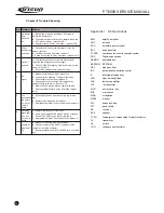
3.3Transmitter (TX) Illustration
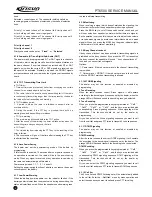
Transmitter Power Amplifier
The modulated signals from VCO are amplified at Q2, Q4, Q59, Q5,
Q3, and then sent to Q1 for power amplification. Q1 output power:
4W.
The Q1 and Q3 gate offset is controlled by APC circuit. Transmitter
output power can be controlled conveniently by changing the gate-
offset.
APC (Auto Power Control) Circuit
R57, R65 and R66 are the amplifier current checker, IC3A is the
sample amplifier of the amplification current; .IC3B is the power
comparison amplifier.
If the transmitter output power is too big, the amplifier current will
increase, IC3A output will mount, IC3B output voltage decrease, the
offset voltage added to Q1 and Q3 will decrease, and then the
transmitter output power will decrease. Vice versa, such can ensure
steady transmitter output power in different working circumstances.
MCU changes the input power to IC3B to set the power.
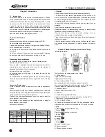
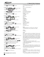
3.4 Frequency Combiner Illustration
Figure 3.4 Frequency Combiner Illustrations
This radio adopts phase locked loop (PLL) type frequency combiner.
The frequency combiner consists of the reference oscillator, voltage
controlled oscillator (VCO), programmable frequency divider, phase
PT6500 SERVICE MANUAL
1
1
2
2
3
3
4
4
D
D
C
C
B
B
A
A
Title
Number
Revisi on
Size
A4
Date:
2007-7-26
Sheet of
File:
X:\PT6500\.. \Frequency confi guration.SchDoc
Drawn By:
ANT
ANT SW
RF AMP
MCF
51.65MHz
IF SYSTEM
CF1
450KHz H
CF2
450KHz F
X3 multi ply
AK2346
AF AMP
TCXO
12.8MHz
MIC AMP
PLL VCO
TX AMP
PA AMP
RX
TX
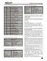
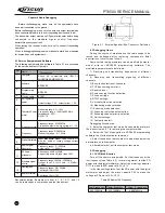
Chapter 3 Electrocircuit
3.1 Frequency Configuration
Figure 3.1 Frequency Structure
This radio adopts the 2nd Mixer, the 1st IF 51.65MHz, the 2nd IF
450kHz.
1
1
2
2
3
3
4
4
D
D
C
C
B
B
A
A
Title
Number
Revision
Size
A4
Date:
2007-7-26
Sheet of
File:
X:\PT6500\..\T X.SchDoc
Drawn By:
RF AMP
5T
5R
Q4
Q5
Q3
DRIVE
DRIVE
PRE
5T
5T
APC
Q12
ANT SW
LPF
APC CONTROL
IC3
TX/RX SW
Q1
RF POWER
APC
5T
SW
BATTARY
7.5V
VCO
ANT
Figure 3.3 Power amplifier and antenna switch schematic diagram
Содержание PT6500
Страница 1: ...PROFESSIONAL TWO WAY RADIO PT6500 V071208 FM PORTABLE RADIO SERVICE MANOAL Welcome ...
Страница 33: ...PT6500 SERVICE MANUAL Figure 1 PT6500 Top Main Board Position Number Diagram 136 174MHz 32 ...
Страница 34: ...PT6500 SERVICE MANUAL Figure2 PT6500 Bottom Main Board Position Number Diagram 136 174MHz 33 ...
Страница 35: ...Figure 3 400 470MHz PT6500 Top Main Board Position Number Diagram 34 PT6500 SERVICE MANUAL ...
Страница 36: ...35 PT6500 SERVICE MANUAL Figure 4 400 470MHz PT6500 Bottom Main Board Position Number Diagram ...
Страница 37: ...Figure 5 PT6500 PTT Top Board Position Number Diagram 36 PT6500 SERVICE MANUAL ...
Страница 38: ...37 PT6500 SERVICE MANUAL Figure 6 PT6500 PTT BOTTOM Board Position Number Diagram ...