16
TK-785
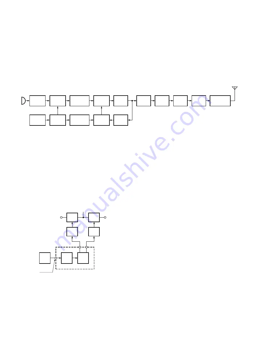
Since a signal output from Q106 is input to the PLL IC, it
passes through CN101 and buffer amplifier (Q300) and goes
to the PLL IC (IC300). The modulation signal from CN101 is
applied to D109 and passes through C125 and C126 to
modulate the carrier.
The PLL IC uses a fractional N type synthesizer to im-
prove the C/N ratio and lock-up speed. The VCO output sig-
nal input to the pin 5 of the PLL IC is divided to produce a
comparison frequency according to a channel step. This sig-
IC508
SHIFT
REG.
IC511
CPU
Q10
SW
Q11
SW
IC300
PLL
Q13
SW
Q12
SW
LD
CONTROL UNIT
T/R
8C
8R
8T
KEY
PLL lock
: LD "H"
Fig. 6
Unlock circuit
CIRCUIT DESCRIPTION
IC504
IC3
Q103
IC711
MIC
AF AMP
TA75S01F
MIC KEY
INPUT
AF AMP,
IDC, LPF
TC35453F
IC511
CPU
30620M8
-394GP
SUM AMP
TA75W558FU
X1
VCXO
16.8MHz
VCO
2SK508NV
(K53)
IC300
PLL
SA7025DK
Q106
RF AMP
2SC4226
(R24)
Q300
BUFFER
2SC4215
(Y)
Q202
RF AMP
2SC4093
(R27)
Q204
RF AMP
2SC3357
Q205
ANT
RF AMP
2SC2954
IC400
POWER AMP
M68706
Q7
BUFFER
2SC5110
(O)
Fig. 5
Transmitter system (M type)
■
Unlock Circuit
During reception, the T/R signal goes high, the KEY signal
goes low, and Q10 turns on. Q11 turns on and a voltage is
applied to the collector (8R). During transmission, the T/R
signal goes low, the KEY signal goes high and Q13 turns on.
Q12 turns on and a voltage is applied to 8T.
The CPU in the control unit monitors the PLL (IC300) LD
signal directly. When the KEY signal goes low, no voltage is
applied to 8T, and no signal is transmitted.
nal is compared with the reference frequency which is out-
put from the VCXO (X1). VCXO provides 16.8MHz, 2.5ppm
(–30 to +60
°
C) and guarantees stable performance when
the temperature changes. The output signal from the phase
comparator passes through a charge pump and an external
active LPF (Q301, Q302) in the PLL IC to generate a DC VCO
control voltage CV. Serial data (DT, CK, EP) are output from
the CPU (IC511) and shift register (IC8) in the control unit to
control the PLL IC.
■
Power Amplifier Circuit (K,E type)
The transmit output signal from the VCO is amplified to a
specified level of the power module (IC400) by the drive
block (Q203, Q204). The amplified signal passes through
the transmission/reception selection diode (D211) and goes
to a low-pass filter. The low-pass filter removes unwanted
high-frequency harmonic components, and the resulting sig-
nal is goes the antenna terminal.
■
Power Amplifier Circuit (M type)
The transmit output signal from the VCO is amplified to a
specified level of the power module (IC400) by the drive
block (Q202, Q204, Q205). The amplified signal passes
through the transmission/reception selection diode (D209)
and goes to a low-pass filter. The low-pass filter removes
unwanted high-frequency harmonic components, and the
resulting signal is goes the antenna terminal.
Содержание TK-785
Страница 69: ...TK 785 TK 785 TK 785 BLOCK DIAGRAM K E 95 ...
Страница 70: ...TK 785 TK 785 TK 785 96 BLOCK DIAGRAM M ...

