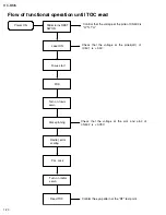


RC-BM5
1-28
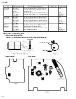
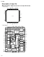
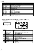
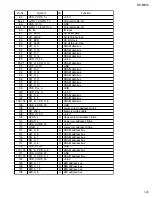
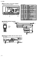
LS188 (IC703) : VCD decoder
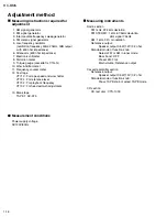
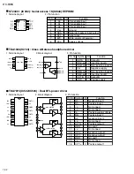
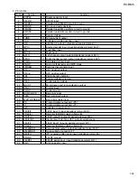
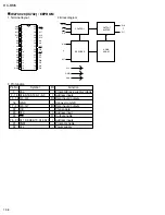
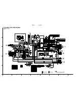
1. Terminal layout
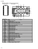
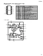
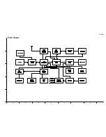
2. Block diagram
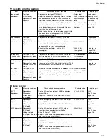
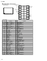
1 to 3,22
4 to 11
12 to15
16
17,18,20,21
19
23,24
25
26
27
28
29
30
31
32
33
34
35
36
37 to 42
43
44,45
46
47
48
49
50
51
52 to 55
56
57,58
59
60,61
EMI_A_9 to EMI_A_12
EMI_D_7 to EMI_D_0
EMI_A_0 to EMI_A_3
VDD_IO_00
EMI_A_4 to EMI_A_7
VSS_IO_00
EMI_A_15 to EMI_A_16
EMI_A_18
I2C_CLK
I2C_DAT
VSS_OSC_0
XTLCLK_I
XTLCLK_O
VDD_OSC_0
TEST_H
RESET_L
HSYNC_L
VSYNC_L
CLK27_O
VDAT_7 to VDAT_2
VSS_CORE_00
VDAT_1 to VDAT_0
VDD_CORE_00
AUD_XCK
AUD_BCK
AUD_LRCK
AUD_DOUT
AUD_DIN
GPIO_23 to GPIO_20
VDD_IO_10
GPIO_19,GPIO_18
VSS_CORE_10
GPIO_17,GPIO_16
O
I
O
-
O
-
O
O
O
-
-
I
O
-
I
I
I
I
O
O
-
O
-
-
O
O
O
I
-
-
-
-
-
EMI address bus
EMI data bus
EMI address bus
+3.3V
EMI address bus
+3.3V
EMI address bus
EMI address bus
I2C clock
I2C data
GND
Crystal input
Crystal output
+3.3V
Test
Hardware reset
Horizontal sync
Vertical sync
CLK 27MHz output
Luminance output
GND
Luminance output
+2.5V
External audio clock
Audio bit clock
Audio left/right clock
Audio data output
Audio data input
Programmable I/O
+3.3V
Programmable I/O
GND
Programmable I/O
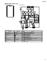
1
38
39
64
128
103
102
65
Pin No.
Symbol
Function
3. Pin function
I/O
DRAM
Interface
EMI
Interface
Prog.I/O
Interface
Host/CD
Interface
RISC
Processor
DSP
Core
Video
Processor
On Screen
Display
Video
Decoder
Audio
Decoder
Audio
Interface
Register
Bank
DRAM
ROM/SRAM
Panel and
keypad
CD
Host
NTSC/PAL
Encoder
Audio
DAC
Audio
ADC
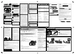
Содержание RC-BM5
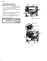
Страница 41: ...RC BM5 2 1 A B C D E F G 1 2 3 4 5 Block diagram ...
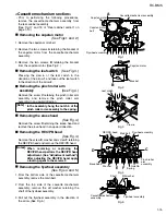
Страница 48: ...RC BM5 2 8 RC BM5 H A B C D E F G 1 2 3 4 5 Printed circuit boards Main board Reverse side ...
Страница 49: ...RC BM5 2 9 A B C 1 2 3 4 5 Tuner board Cassette board Reverse side Reverse side ...
Страница 50: ...RC BM5 2 10 A B C D 1 2 3 4 5 Display board Reverse side Power amplifier board Reverse side ...
Страница 51: ...RC BM5 2 11 A B C 1 2 3 4 5 Volume switch board Reverse side Phone jack board Reverse side ...