background image

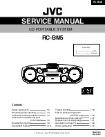
RC-BM5

1-14

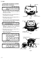
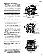
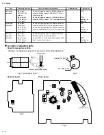
CD pickup cover

CD mechanism assembly

A

A

A

Fig.1

CD pickup unit

CD pickup unit

B

B

Shaft

Sliding Spring

Slit washer

Feed middle gear

Fig.2

Removing the CD pickup unit

(See Figs. 1 to 2.)

1.

2.

3.

4.

Remove the three screws 

A

 retaining the CD 

pickup cover.

Remove the slit washer retaining the feed middle 
gear and take out the feed middle gear.

Loosen the two screws 

B

 retaining the shaft and 

pull out the shaft in the direction of the arrow.

Take out the CD pickup unit.

<CD mechanism section>

[Note]

In the assembly, be sure to attach the 
sliding spring in the correct orientation 
before attaching the CD pickup unit.

(See Fig.2.)

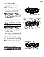
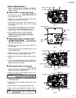
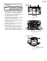
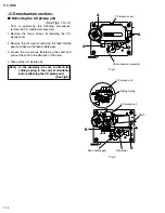
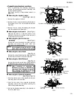
Prior to performing the following procedures, 
remove the CD mechanism assembly.

Содержание RC-BM5

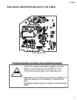
Страница 1: ... products Importance administering point on the safety Disassembly method Adjustment method 1 2 1 3 1 4 1 5 1 6 1 16 RC BM5 Area suffix J U S A C Canada Trouble shooting Flow of functional operation until TOC read Maintenance of laser pickup Replacement of laser pickup Description of major ICs Wiring connection 1 19 1 20 1 21 1 21 1 22 1 37 CD PORTABLE SYSTEM ...

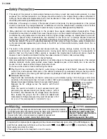
Страница 2: ...uct antenna terminals knobs metal cabinet screw heads headphone jack control shafts etc to be sure the product is safe to operate without danger of electrical shock Do not use a line isolation transformer during this check Plug the AC line cord directly into the AC outlet Using a Leakage Current Tester measure the leakage current from each exposed metal parts of the cabinet particularly any expose...

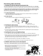
Страница 3: ... as a conductive sheet or an iron plate over it before placing the traverse unit optical pickup on it 2 1 Ground the workbench 2 2 Ground yourself Use an anti static wrist strap to release any static electricity built up in your body In order to maintain quality during transport and before installation both sides of the laser diode on the replacement optical pickup are shorted After replacement re...

Страница 4: ... switches malfunction the laser is able to function 6 CAUTION Use of controls adjustments or performance of procedures other than those specified herein may result in hazardous radiation exposure VARNING Osynlig laserstrålning när denna del är öppnad och spårren är urkopplad Betrakta ej strålen VARO Avattaessa ja suojalukitus ohitettaessa olet alttiina näkymättömälle lasersäteilylle Älä katso säte...

Страница 5: ...fusible de surete par le meme type 2 5A 250V pour F201 Ce symbole specifie le type du fusible a fonctionnement rapide Caution For continued protection against risk of fire replace only with same type 2 5A 250V for F201 This symbol specifies type of fast operating fuse Power amplifier board F201 CN204 CN206 CN203 ...

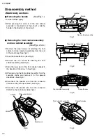
Страница 6: ...om the rear of the main body See Fig 2 Open the cassette door See Fig 3 Remove the two screws B retaining the front cabinet assembly See Fig 3 Slide the lower part of the front cabinet slightly in the direction of the arrow 1 See Fig 4 While removing the front cabinet assembly from the cassette knobs and remove it in the upward direction 2 See Fig 4 Disconnect the speaker wire from the connector C...

Страница 7: ...ws D retaining the right and left main speaker assemblies Remove the solders from the soldered sections b and c of the right and left main speaker assemblies remove the wires Take out the right and left main speaker assemblies Removing the right and left sub speaker assemblies See Fig 7 1 2 3 From the inside of the front cabinet assembly remove the four screws E retaining the right and left sub sp...

Страница 8: ...door Removing the cassette door bracket See Figs 10 and 11 1 2 3 While pressing the sections i on the left and right of the cassette door bracket in the direction of the arrow 1 remove the cassette door bracket from the bosses j of the front cabinet assembly and then open the cassette door bracket in the direction of the arrow 2 Press the section k of the cassette door bracket and remove the casse...

Страница 9: ...to performing the following procedures remove the front cabinet assembly from the rear cabinet assembly Removing the power amplifier board and phone jack board See Fig 14 1 2 3 4 5 6 Disconnect the wire from the connector CN206 on the power amplifier board Disconnect the wire from the connector CN801 on the main board Remove the wire from the soldered section r on the power amplifier board Remove ...

Страница 10: ...tuner board See Fig 17 Removing the cassette deck mechanism assembly and cassette board See Figs 18 and 19 1 2 3 4 5 6 Remove the three screws Q and screw Q retaining the cassette deck mechanism assembly Lift the cassette deck mechanism assembly slightly and move it as shown in Fig 19 Remove the three screws R retaining the cassette board Lift the cassette board slightly remove the capstan motor w...

Страница 11: ... from the connector H402 on the volume switch board See Fig 12 Disconnect the wire from the connector CN206 on the power amplifier board See Fig 14 Disconnect the wire from the connector CN801 on the main board See Fig 14 Disconnect the wire from the connector H801 on the tuner board See Fig 16 Remove the four screws T retaining the CD Cassette mechanism assembly See Fig 21 Slide the CD Cassette m...

Страница 12: ... board be careful not to scratch or damage the CD door CD Cassette mechanism section Caution Be sure to solder the short land section ab on the CD pickup unit before disconnecting the card wire from the CD pickup unit If the card wire is disconnected without applying solder the CD pickup may be destroyed by static electricity 8 After soldering disconnect the card wire from the CD pickup unit and t...

Страница 13: ...Press the claws ad of the CD open knob in the direction of the arrow 3 and then take out the CD open knob from the top side of the CD tray assembly Prior to performing the following procedures remove the main board from the CD Cassette mechanism assembly From the bottom side of the CD Cassette mechanism assembly remove the four screws W retaining the CD mechanism assembly Removing the CD door swit...

Страница 14: ...kup cover Remove the slit washer retaining the feed middle gear and take out the feed middle gear Loosen the two screws B retaining the shaft and pull out the shaft in the direction of the arrow Take out the CD pickup unit CD mechanism section Note In the assembly be sure to attach the sliding spring in the correct orientation before attaching the CD pickup unit See Fig 2 Prior to performing the f...

Страница 15: ...f the cassette mechanism assembly remove the main belt From the top side of the cassette mechanism assembly remove the slit washer retaining the shaft of the flywheel assembly Pull out the flywheel assembly in the direction of the arrow See Fig 5 Removing the flywheel assembly See Figs 4 and 5 Cassette mechanism section Removing the leaf switch See Fig 3 Pressing the claw a of the leaf switch in t...

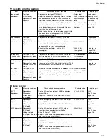
Страница 16: ...ed and wow flutter VT724 For reference level VT702 For playback frequency VT702 For head azimuth adjustment 13 Blank tape TAPE AC 225 Measurement conditions Power supply voltage AC120V 60Hz Measuring instruments Radio section FM 1kHz 22 5kHz deviation FM STEREO 1kHz 67 5kHz deviation pilot signal 7 5kHz AM 1kHz 30 modulation Reference output Speaker output 0 5W 1 2V 3 2 ohm Standard mode of functi...

Страница 17: ... emphasis Signal output terminal Speakers Head azimuth adjustment Tape speed and wow flutter check and adjustment PB frequency response check Bias frequency check REC and PB frequency response adjustment 1 2 3 1 2 3 Output level Within 2dB 2dB of maximum output level Phase difference R and L channels Minimum 2940 to 3090Hz Within 0 38 unweighted Deviation between 1kHz and 8kHz 0 3dB 6dB Level diff...

Страница 18: ...output Set the FM signal generator at 90MHz and the unit receiving 90MHz adjust L101 for maximum output Set the FM signal generator at 106MHz and the unit receiving 106MHz adjust TC102 for maximum output Set the AM signal generator at 98MHz with stereo deviation and the unit receiving 98kHz Adjust VR101 so that the separation between the R and L channels for maximum Signal input AM ANT COIL antenn...

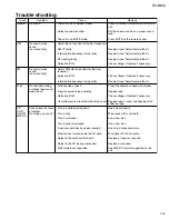
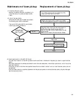
Страница 19: ...pported No sound No sound weak sound Low sensitivity No sound weak sound Low sensitivity No sound recording unsteady tape sound weak sound Cannot read the table of content No display no sound General AM FM Tape CD CD R CD RW MP3 CD Remedy Press STANDBY ON button to turn on the unit Set the volume control to a proper sound level Press MUTE on the remote control Readjust see Adjustment method Readju...

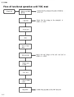
Страница 20: ...he voltage at the pin5 of CN502 is H L H Check that the voltage at the pin64 LD of IC501 is 3 3V Focus start FOK PLL Lock Turn on radial servo Read TOC Confirm the eye pattern at the RF test point Turn on focus servo Disc spinning Radial_error scaling Check that the voltage at the pin1 and pin2 of CN502 is 0 78V ...

Страница 21: ...hen the life of the laser diode has expired the following symptoms will appear The level of RF output EFM output ampli tude of eye pattern will below Is the level of RF OUT under 1 25V 0 22Vp p Replace it NO YES O K 3 Semi fixed resistor on the APC PC board The semi fixed resistor on the APC printed circuit board which is attached to the pickup is used to adjust the laser power Since this adjustme...

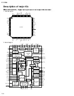
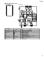
Страница 22: ... 31 44 SELPLL CRIN CROUT CL16 CL11 4 24 16 15 26 49 48 47 46 45 SBSY SFSY SUB RCK 43 STATUS RESET 38 63 34 61 62 V1 V2 V3 V4 V5 KILL 32 KILL PEAK DETECT 23 22 19 18 21 20 RP RN LP LN VPOS Vneg 36 35 37 SDI WCLI SCLI 30 29 28 27 EF SCLK WCLK DATA DOBM 51 ERROR CORRECTOR FLAGS 53 CFLG 59 60 MOTO1 MOTO2 64 LDON 56 55 54 SL FO RA 1 2 3 4 5 6 7 8 9 10 11 12 13 14 15 16 17 18 19 20 21 22 23 24 25 26 27 ...

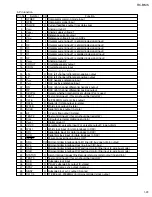
Страница 23: ... output DAC left channel differential positive output DAC negative reference input DAC positive reference input DAC right channel differential negative output DAC right channel differential positive output Selects whether internal clock multiplier PLL is used Test control input 1 this pin should be tied LOW 16 9344MHz system clock output Serial d4 1 data output 3 state Word clock output 3 state Se...

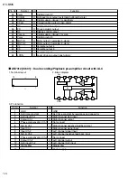
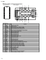
Страница 24: ...drain AN7312 IC601 Dual recording Playback pre amplifier circuit with ALC 1 Terminal layout 3 Pin function 2 Block diagram 1 7 14 8 1 2 3 4 5 6 7 8 9 10 11 12 13 14 GND ALC time constant ALC input Ch 1 Output Ch 1 Phase compensation Ch 1 N E B Ch 1 Input Ch 1 Input Ch 2 N E B Ch 2 Phase compensation Ch 2 Output Ch 2 ALC input Ch 2 Ripple filter Vcc GND ALC time constant by resistance and capacitor...

Страница 25: ... order address bits Data input output Chip enable input Output enable input Write enable input Program supply voltage 12 5 13volts Flash mode selection Power supply voltage 5V Ground pin Function 2 Block diagram PORT 0 DRIVERS PORT2 DRIVERS RAM PORT 0 LATCH PORT 2 LATCH ROM ACC B REGISTER TMP2 TMP1 PSW STACK POINTER T0 T1 T2 SFRs TIMERS PORT1 LATCH osc PORT1 LATCH PORT1 DRIVERS DPTR PROGRAM COUNTE...

Страница 26: ...ight channel input 2 Right channel input 1 Left channel loudness input Left channel input 4 Left channel input 3 Left channel input 2 Left channel input 1 Audio processor left channel input Gain output and input selector for left channel Left channel input for bass controller Left channel output for bass controller Right channel input for bass controller Right channel output for bass controller Ri...

Страница 27: ...ut Power 5V 0 5V Input output Not connect Read write control Row address strobe Not connect Address inputs Power 5V 0 5V Ground Address inputs Output enable Column address strobe upper byte Column address strobe lower byte Not connect Input output Ground Input output Ground Pin No Symbol Function I O I O I I O I O I O I O CONTROL LOGIC CLOCK GENERATOR REFRESH CONTROLER REFRESH COUNTER ROW ADDRESS ...

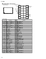
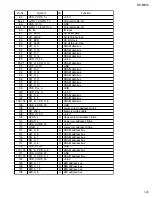
Страница 28: ..._17 GPIO_16 O I O O O O O I O I I I I O O O O O O I EMI address bus EMI data bus EMI address bus 3 3V EMI address bus 3 3V EMI address bus EMI address bus I2C clock I2C data GND Crystal input Crystal output 3 3V Test Hardware reset Horizontal sync Vertical sync CLK 27MHz output Luminance output GND Luminance output 2 5V External audio clock Audio bit clock Audio left right clock Audio data output ...

Страница 29: ...0 DR_A_3 DR_A_4 VDD_CORE_30 EMI_A_17 EMI_A_14 EMI_A_13 EMI_A_8 I I I I I O O O O O O O O O O O O O O O O 2 5V Programmable I O GND Programmable I O IR input CD serial data CD left right clock CD bit clock CD data error flag DRAM data bus DRAM data bus DRAM data bus DRAM data bus 2 5V DRAM data bus GND DRAM data bus DRAM data bus DRAM data bus DRAM data bus DRAM data bus DRAM data bus GND 2 5V DRAM...

Страница 30: ...ier T S D 1 2 3 4 5 6 7 8 9 10 11 12 13 14 15 BS 30K 30K Vcc ST BY 45 45 GND Power GND1 Pre GND2 Pre 30K 30K N C BS OUT1 Vcc OUT2 BS POWER GND ST BY FILTER RF1 IN2 IN1 RF2 PRE GND1 PRE GND2 FILTER BS 1 Terminal layout NJM7805FA IC505 Regulator 1 INPUT 2 OUTPUT 3 GND 2 Block diagram BANDGAP REFERENCE 1 INPUT THERMAL SHUTDOWN OVER VOLTAGE PROTECTION SOA PROTECTION SHORT CIRCUIT PROTECTION 3 GND 2 OU...

Страница 31: ...in Data output pin Chip enable pin Synchronization clock input pin Din transistor input pin 3 Pin function Pin No Symbol I O Function KO6 K11 K12 K13 K14 K15 TEST VDD VDD1 VDD2 VSS OSC DO CE CLK DI KEY SCAN OSC DO DI CLK CE VDD VDD1 VDD2 VSS TEST 49 50 51 52 53 54 55 56 57 58 59 60 61 62 63 64 32 31 30 29 28 27 26 25 24 23 22 21 20 19 18 17 SG32 SG31 SG30 SG29 SG28 SG27 SG26 SG25 SG24 SG23 SG22 SG...

Страница 32: ...c OUT1 n c GND1 OUT1 OUT2 n c GND2 OUT2 VDD 2 IN1 IN1 n c n c Vp IN2 IN2 n c OUT2 GND2 n c OUT2 OUT1 GND1 n c OUT1 Negative input 1 Positive input 1 Not connect Not connect Positive supply voltage Positive input 2 Negative input 2 Not connect Positive output 2 Ground 2 Not connect Negative output 2 Negative output 1 Ground 1 Not connect Positive output 1 I I I I O O O O Pin No Symbol I O Function ...

Страница 33: ...DJ CMFB RFFB RFEQO EQSEL LD VDD L CFIL MON DIN GND PWRON CMFB RFFB RFEQO CDRW EQSEL VDD RGADJ Current output to laser diode Laser supply voltage External filter capacitor Laser monitor diode input Central diode input Ground Power on select input Common mode feedback voltage input External RF feedback resistor RF amplifier output Gain select input for CD A V CD R W Equalizer speed select input n 1 ...

Страница 34: ... STABILIZER SHIFT REGISTER MULTIPLEXER PLL DECODER MATRIX SDS MUTE STATUS REGISTER IN LOCK DETECTOR CHARGE PUMP AFC AM FM INDICATOR 28 27 29 3 5 39 37 35 33 17 18 SEQUENTIAL CIRCUIT PRESCALER LAST STATION MEMORY CRYSTAL OSCILLATOR AM FRONT END PROGRAMMABLE COUNTER WINSOW DETECTOR 38 34 7 23 1 AM OSCILLATOR AM IF AM MIXER 25 26 31 30 2 6 AGC AM DETECTOR FM AM Up Down Level 19 kHz V I CONVERTER 4 11...

Страница 35: ...input input impedance typical 150k Loop filter input Mute input Left channel output output impedance typical 4 3k Right channel output output impedance typical 4 3k Pilot detector filter input Grond of IF detector and MPX stage Ceramic discriminator input AFC negative output AFC positive output Field strength indicator Supply voltage for tuning Digital supply voltage Mono stereo and tunig indicati...

Страница 36: ... Q1 15 Q4 18 Q2 16 Q3 17 GND PGM CE OE CONTROL OUTPUT BUFFER DECODER CORE ARRAY A0 A17 Vcc GND Vpp Q0 Q7 Vpp A16 A15 A12 A7 A0 Q0 Q2 GND Q3 Q7 CE A10 OE A11 A9 A8 A13 A14 A17 PGM Vcc Program Erase supply voltage Address inputs Data inputs outputs Connect to GND Data inputs outputs Chip enable Address input Output enable Address inputs Program enable Power supply I I O I O I O I Pin No Symbol I O F...

Страница 37: ... board Forward side OW25 61080 01 Power amplifier board Forward side CN204 CN206 CN203 OW31 20190 50 OW31 20190 56 BATT AC SOCKET OW31 20160 52 OW31 20160 54 OW25 94060 03 OW20 42042 08 OW31 60080 54 OW31 60090 52 4U7 50V OW31 60080 54 OW31 60090 52 4U7 50V Volume switch board Forward side H402 Display board Forward side CN401 LED41 OW32 30140 20 OW20 41102 32 CN601 CN602 CN603 Cassette board Forw...

Страница 38: ...RC BM5 VICTOR COMPANY OF JAPAN LIMITED AUDIO COMMUNICATION BUSINESS DIVISION PERSONAL MOBILE NETWORK BUSINESS UNIT 10 1 1Chome Ohwatari machi maebashi city 371 8543 Japan 200210 No 21129 ...

Страница 39: ...IGHT 2002 VICTOR COMPANY OF JAPAN LTD SCHEMATIC DIAGRAMS Contents Block diagram Standard schematic diagrams Printed circuit boards 2 1 2 2 2 8 11 CD ROM No SML200210 RC BM5 Area suffix J U S A C Canada RC BM5 CD PORTABLE SYSTEM ...

Страница 40: ... on the silk screen printed side parts side of the PWB diagrams the parts that are printed over with black such as the resistor diode and ICP or identified by the mark nearby are critical for safety This regulation does not correspond to J and C version ...

Страница 41: ...RC BM5 2 1 A B C D E F G 1 2 3 4 5 Block diagram ...

Страница 42: ...01 Voltage chart PIN1 PIN2 PIN3 8 4 V 0 V 5 V IC505 NJM7805 PIN1 PIN2 PIN3 PIN4 PIN5 6 PIN7 PIN8 11 PIN12 PIN13 15 7 15 V 0 V 3 49 V 3 48 V 3 49 V 3 5 V 3 48 V 3 5 V 3 48 V IC801 PT2314 PIN16 PIN17 18 PIN19 22 PIN23 PIN24 PIN25 PIN26 PIN27 PIN28 3 49 V 3 48 V 3 49 V 3 48 V 3 48 V 0 V 4 2 V 4 25 V 3 49 V Voltage chart Q301 C1383 E B C 4 84 V 5 48 V 11 33 V Voltage chart Q302 945 0 V 0 6 V 0 V Q303 ...

Страница 43: ... 0 58 V 0 32 V 0 58 V PIN32 PIN33 PIN34 PIN35 PIN36 PIN37 PIN38 PIN39 PIN40 PIN41 PIN42 PIN43 PIN44 PIN45 PIN46 PIN47 PIN48 PIN49 PIN50 PIN51 PIN52 PIN53 PIN54 PIN55 PIN56 PIN57 61 PIN62 PIN63 PIN64 PIN65 PIN66 PIN67 PIN68 PIN69 PIN70 PIN71 PIN72 PIN73 PIN74 PIN75 PIN76 PIN77 PIN78 PIN79 PIN80 PIN81 PIN82 PIN83 PIN84 PIN85 PIN86 PIN87 PIN88 PIN89 PIN90 PIN91 PIN92 PIN93 PIN94 PIN95 PIN96 PIN97 PIN...

Страница 44: ...N30 31 PIN32 PIN33 PIN34 PIN35 PIN36 PIN37 PIN38 0 V 1 37 V 0 69 V 1 37 V 0 64 V 1 37 V 0 54 V 1 27 V PIN39 PIN40 41 PIN42 PIN43 PIN44 0 99 V 1 27 V 0 V 0 75 V 0 21 V Q106 557B E B C 0 V 5 44 V 4 82 V Voltage chart Q107 547B 4 83 V 0 5 V 0 V Q108 547B 4 86 V 0 V 0 V Q109 547B 0 V 0 V 0 5 V Q102 2SA733P E B C 6 34 V 5 49 V 6 31 V Voltage chart Q103 2SC945 0 V 0 V 0 V To F 5 on page 2 2 To C 5 on pa...

Страница 45: ...PIN14 0 V 3 41 V 1 35 V 1 24 V 0 01 V 1 24 V 1 35 V 3 4 V 0 V 6 78 V 6 82 V IC601 AN7312 Voltage chart Q601 945 E B C 0 V 0 V 0 V Voltage chart Q602 945 0 V 0 V 0 V Q603 945 0 V 0 6 V 0 V Q604 945 0 V 7 6 V 7 65 V Q605 945 0 V 0 V 0 V To A 2 and A 3 on page 2 2 Cassette section CON61 CN601 CN603 CN602 CN604 TO MAIN PCB CN803 ...

Страница 46: ...PIN16 21 PIN22 PIN23 26 2 4 V 2 41 V 2 4 V 2 45 V 2 41 V 2 45 V 2 41 V 2 45 V 0 V 2 41 V 2 42 V 2 41 V IC401 PT6553 PIN27 PIN28 45 PIN46 49 PIN50 55 PIN56 PIN57 PIN58 59 PIN60 PIN61 PIN62 PIN63 PIN64 2 45 V 2 41 V 4 87 V 0 V 4 87 V 2 31 V 0 V 3 89 V 4 85 V 0 V 4 83 V 0 V Voltage chart PIN1 2 PIN3 4 6 V 0 V IC402 RPM6938 To G 3 and G 4 on page 2 2 ...

Страница 47: ... PIN9 PIN10 15 0 V 14 75 V 4 77 V 14 18 V 0 V 7 99 V 0 V IC201 BA5417 Voltage chart Q201 8050D E B C 0 V 0 V 0 V Voltage chart Q202 8050D 0 V 0 V 0 V Q203 2SC945 0 6 V 0 V 2 87 V Q204 928 1 4 V 13 8 V 13 4 V Q205 1913 13 52 V 12 5 V 0 V Q206 8050D 0 V 13 8 V 12 5 V Q207 2SC945 13 2 V 13 9 V 13 8 V To G 2 on page 2 2 To G 2 on page 2 2 CN206 CN204 CN203 CN205 CN202 CN201 FROM MAIN PCB CN801 FROM MA...

Страница 48: ...RC BM5 2 8 RC BM5 H A B C D E F G 1 2 3 4 5 Printed circuit boards Main board Reverse side ...

Страница 49: ...RC BM5 2 9 A B C 1 2 3 4 5 Tuner board Cassette board Reverse side Reverse side ...

Страница 50: ...RC BM5 2 10 A B C D 1 2 3 4 5 Display board Reverse side Power amplifier board Reverse side ...

Страница 51: ...RC BM5 2 11 A B C 1 2 3 4 5 Volume switch board Reverse side Phone jack board Reverse side ...

Страница 52: ...VICTOR COMPANY OF JAPAN LIMITED AUDIO COMMUNICATION BUSINESS DIVISION PERSONAL MOBILE NETWORK BUSINESS UNIT 10 1 1Chome Ohwatari machi maebashi city 371 8543 Japan 200210 No 21129SCH RC BM5 ...

Отзывы: