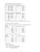

14
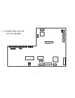
5.1
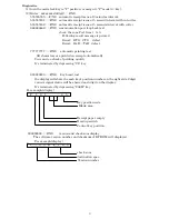
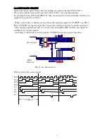
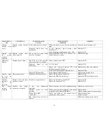
CONNECTOR TABLE
CN1
CN2
CN4
CN5
CN6
DRAWER
POWER
SCOM0
SCOM1
SCOM2
PIN signal
PIN signal
PIN signal
PIN signal
PIN signal
1
+24V
1 GND
1
SG
1
SG
1
SG
2
DRW
2 GND
2
TxD
2
TxD
2
TxD
3
DRW SOL
3 +24V
3
RxD
3
RxD
3
RxD
4
SG
4 +24V
4
RTS
4
RTS
4
RTS
5
CTS
5
CTS
5
CTS
6
Vcc
6
DTR
6
DTR
7
DSR
7
DSR
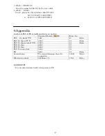
CN3
CN8
CN9
CN10
display
MOTOR
Paper end
Head up SW
PIN signal
PIN signal
PIN signal
PIN
PIN signal
1
DET1
11 DSP G2
1
1A
1
LED
1 HS
2
DSP A
12 DSP G3
2
2A
2
SG
2 SG
3
DSP B
13 DSP G4
3
1B
3
NEND
3 NC
4
DSP C
14 DSP G5
4
2B
4
SG
5
DSP D
15 DSP G6
CN13
6
DSP E
16 DSP G7
CN11
CN12
key return
7
DSP F
17 DSP G8
CUTTER SW
Paper NEND
PIN signal
8
DSP G
18 DSP G9
PIN signal
PIN signal
1
KR0
9
DSP P
19 DSP G10
1
CTSW
1
LED
2
KR1
10 DSP G1
20 DET2
2
SG
2
SG
3
KR2
3
NEND
4
KR3
5
KR4
CN7
HEAD
CN14
CN15
CN16
PIN signal
PIN signal
control lock
key scan
down load
1
VH
15 GND
PIN signal
PIN signal
PIN signal
2
VH
16 GND
1
COM
1 KS0
1
Vcc
3
VH
17 GND
2
REG
2 KS1
2
BUSY
4
VH
18 GND
3
X
3 KS2
3
CLK1
5
DI
19 TM1
4
Z
4 KS3
4
RxD1
6
/STB2
20 /STB1
5
P
5 KS4
5
CE
7
/STB3
21 NC
6
SP
6 KS5
6
EPM
8
VDD
22 /LAT
7 KS6
7
GND
9
TM2
23 CLK
8 KS7
8
RESET
10 GND
24 DO
9 KS8
9
CNVSS
11 GND
25 VH
10
TxD1
12 GND
26 VH
13 GND
27 VH
14 GND
28 VH


