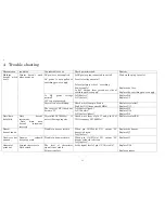
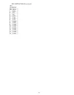


12
PHENOMEN
ON
CONDITION CONSIDERABLE
CAUSE
CHECK POINT/
METHOD
REMEDY
Is the head unit over heat?
When the head is over heated, printing is
stop.
Wait for head becomes cool.
Printer
doesn’t work
at all
Printer motor doesn’t
rotate
Stepping signal does not
generated.
Is the stepping signal output from
P11X(U11)?
Is the stepping signal output from U18
Replace U11
Replace U18
Printer feed
the paper
without
printing
Printer motor does
work correctly
DC power for print head
unit is not output
When pin12(P142) of U11 outputs “H” ,
the head become active.
Replace Q3,Q4.
The FPC for CPU and FD
units connection is broken
Check conduction of FPC.
Replace FPC
Segment signal is not
generated
Is U14 defect?
Replace U14
Check the voltage between VF1 and
VF2(tolerance3.46Vrms)
Replace converter transformer
Is the cathode voltage of PD14-23.5V?
Replace PD14.
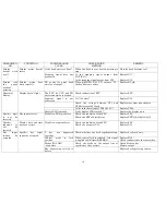
Abnormal
display
Display doesn’t light
Display PCB is broken.
Is the display PCB cracked?
Replace the display unit
Specific digit
is not lit
correctly
Key input correct
Trouble in FD digit driver.
Check the condition of the FPC
Check the FET of digit driver.
Replace FPC
Replace FET(Q2~Q6,Q10~Q14
Specific
segment is
not lit
correctly
Display data and time
data are correct.
Trouble in segment drive.
Check the condition of the FPC.
Check the output of U14
Replace FPC
Replace U14
2 key are depressed
together
Check whethe r any key keeps depressing. Replace key board unit.
Control mode is lock
position
When control lock is released, lock signal
is applied to KR lines(KR0-KR4)
Replace D10
Check conduction of the control key.
Diodes (D14-D23)
are defect.
Check the diode on the output line of
specific key’s key matrix.
Check diode on key
Matrix output.
Key input
cannot be
accepted
Specific key input
cannot be accepted.
Key depressing section is
defect.
Replace key depressing section


