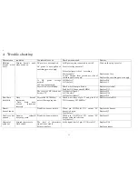
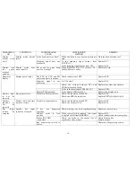

5
C46
104C
10
11
U12E
SN74LV14APW_VBB
+
-
BT1
3/V 280R
R5
122
R43
103
1
TP2
TEST POINT
1
TP3
TEST POINT
R42
103
C47
104C
R44
103
10
11
U10E
SN74LV14APW
12
13
U12F
SN74LV14APW_VBB
1
2
3
4
CN2
B4P-VH
D2
HZU15B2
VOUT
1
MNURST
2
VCC
3
GND
4
U9
PST591CMT
12
13
U10F
SN74LV14APW
C3
104C
R3
122
D3
HZU4.3B2
1
TP1
TEST POINT
nPF
nRESET
VCC
+24V
+24V
VCC
VCC
VBB5
VBB5
nRESET-VBB
8
9
U12D
SN74LV14APW_VBB
6
5
U12C
SN74LV14APW_VBB
VBB5
VBB5
VOUT
1
VIN
2
CB
3
FB
6
NC
5
GND
4
ON/
OFF
7
U1
LM2676S-5.0
C5
103C
D4
EC31QS06
C6
UPW1H471MHH
C7
UPW1V471MPH
L1
SLF12565T-470M2R4
R11
561
R10
221
R9
OPEN
VOUT
8
VIN
7
CB
1
FB
4
NC
2
GND
6
ON/OFF
5
NC
3
U2
LM2675M-5.0
C9
103C
D7
EC31QS06
C8
UPW1H471MHH
C13
UPW1V101MPH
+5VSUB
D6
CMS06
D5
CMS06
R8
100
C4
16V100u LL
VBB
VCC
C10
16V100u LL
RESET-VBB
FL1
DSS9ND31H223
FB5
BLM21PG600SN1
L2
SLF12565T-470M2R4
8
9
U10D
SN74LV14APW
4
3
U10B
SN74LV14APW
6
5
U10C
SN74LV14APW
2
1
U10A
SN74LV14APW
4
3
U12B
SN74LV14APW_VBB
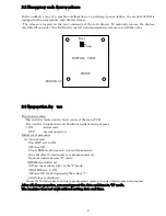
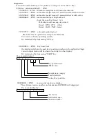
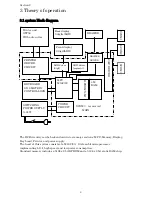
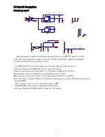
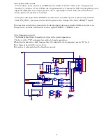
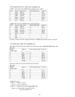
3.2 circuit description
3.2.1 power circuit
After passing through the switching regulator. There is a +24V DC power via CN2.
+24V power is supplied to printer circuit. On the other hand, it’s supplied to regulator
circuit too. There are two regulator circuit.
U1(LM2676S-5.0) is used for logic circuit and for memory back up circuit.
+24V pass through U1(LM2676S-5.0) b5V steady.
During normal operation, the voltage of Vbb line is supplied by +5V line.
Rechargeable current is applied to rechargeable battery via R8.
When AC power is removed, the +5V line decreases, and D5 is turn OFF.
Then the battery supplies Vbb line. And back up the memory contents of RAM chip and CPU
Internal RAM
D5 is used to avoid reverse current when power OFF.
U2(LM2675M-5.0) is used for communication circuit.
+24V pass through U2(LM2675M-5.0) 5V steady.


