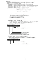
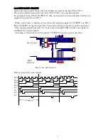
background image


8


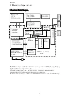
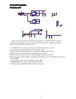
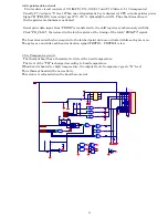
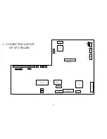
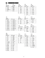
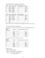
3.2.4. display circuit 
Display signals are applied to display circuit board via CN3. 
The display signals for digit indication are supplied from P120 to P127 and P145,P146 of CPU ports. 
The digit indication signals are amplified at 9 FETs.(2SJ208) And they are supplied to LED common 
terminal on FD and supplied to RI ones. 
The segment data signals are amplified at U14’(M54583) and supplied to segment line of FD and RI 
circuit board. 
 
 From CPU 
  board 


 segment 
  signal 

 for RI 

 digit signal 
      for RI 


DET1

1

DSP A

2

DSP B

3

DSP C

4

DSP D

5

DSP E

6

DSP F

7

DSP G

8

DSP P

9

DSP G1

10

DSP G2

11

DSP G3

12

DSP G4

13

DSP G5

14

DSP G6

15

DSP G7

16

DSP G8

17

DSP G9

18

DSP G10

19

DET2

20

CN3

52045-2010

11

10

2
3
4
5
6
7
8
9

19
18
17
16
15
14
13
12

U14

M54583FP

VCC

VCC

VCC

2

3

4

5

7

8

9

1

10

6

RA1
RA103

R7
103

R6
103

VCC

R39

102

R38

102

R37

102

R36

102

R35

102

R34

102

R33

102

R32

102

R30

102

R29

102

DSPG1

DSPG2

DSPG3

DSPG4

DSPG5

DSPG6

DSPG7

DSPG8

DSPG9

DSPG10

DSPG[1..10]

DSPG[1..10]

FB62

BLM21AG121SN1

FB47

BLM21PG600SN1

FB46

BLM21PG600SN1

FB49

BLM21PG600SN1

FB48

BLM21PG600SN1

FB51

BLM21PG600SN1

FB50

BLM21PG600SN1

FB53

BLM21PG600SN1

FB52

BLM21PG600SN1

FB55

BLM21PG600SN1

FB54

BLM21PG600SN1

FB57

BLM21AG121SN1

FB56

BLM21AG121SN1

FB59

BLM21AG121SN1

FB58

BLM21AG121SN1

FB61

BLM21AG121SN1

FB60

BLM21AG121SN1

FB63

BLM21AG121SN1

DSPS[1..8]

DSPS[1..8]

DSPS1
DSPS2
DSPS3
DSPS4
DSPS5
DSPS6
DSPS7
DSPS8

FB45
BLM21PG600SN1

C54
103C

C52
103C

C48
103C

C63
103C

C26
103C

C62
103C

C73
103C

C72
103C

C70
103C

74LV00A

74LV14A

74LV14A

74LV32A

74LV32A

74LV123A

74LV138A

74LV138A

LMV358

C66
103C

LM393

VBB

VBB

VCC

VCC

VCC

VCC

VCC

VCC

VCC

VCC

8PIN

7PIN

7PIN

7PIN

7PIN

7PIN

8PIN

8PIN

8PIN

4PIN

8PIN

4PIN

16PIN

16PIN

16PIN

14PIN

14PIN

14PIN

14PIN

14PIN

2

1

3

Q14

2SJ208

2

1

3

Q6

2SJ208

2

1

3

Q13

2SJ208

2

1

3

Q5

2SJ208

2

1

3

Q12

2SJ208

2

1

3

Q4

2SJ208

2

1

3

Q11

2SJ208

2

1

3

Q3

2SJ208

2

1

3

Q10

2SJ208

2

1

3

Q2

2SJ208


Содержание J3500E

Страница 1: ...CTRONIC CASH REGISTER J3500E SERVICE MANUAL DOCUMENT No 5190 02 03 REV 01 TITLE J3500E SERVICE MANUAL DRAW CHECK APPR PREPARED BY K SAKAUE 2004 12 6 APPROVED BY COPY RIGHT 2004 BY JAPAN CASH MACHINE C...

Страница 2: ...3 1 system block diagram 4 3 2 circuit description 5 3 2 1 power circuit 5 3 2 2 PF CIRCUIT 6 3 2 3 KEY BOARD CIRCUIT 7 3 2 4 display circuit 8 3 2 5 printer drive circuit 9 3 2 6 Comparator circuit...

Страница 3: ...y As described in table 2 1 If damage is found contact the freight carrier and file a claim promptly If any parts are missing contact JCM within one week of receiving the ECR Initial inspection Perfor...

Страница 4: ...in PCB It is used for initialization and hardware configuration purposes 1 ON initial reset OFF normal operation Initial reset procedure a Initial reset 1 set DIP sw1 to ON 2 Power ON Clears RAM work...

Страница 5: ...7777 NS automatic printing test All characters are printed on receipt automatically You can do a check of printing quality It s terminated by depressing CL key 888888888 NS key board test the display...

Страница 6: ...processor implementing L S I high speed and low power consumption Standard memory includes a 512k x 8 bit EPROM and a 512k x 8 bit static RAM chip Printer unit GTP58 With auto cutter Front display 9 d...

Страница 7: ...D31H223 FB5 BLM21PG600SN1 L2 SLF12565T 470M2R4 8 9 U10D SN74LV14APW 4 3 U10B SN74LV14APW 6 5 U10C SN74LV14APW 2 1 U10A SN74LV14APW 4 3 U12B SN74LV14APW_VBB 3 2 circuit description 3 2 1 power circuit...

Страница 8: ...U12 11 become 3 3V the output of U12 12 nPF turn H Then system goes to operation mode Power OFF When AC input turn OFF the level of U12 11 fall to 0V When input voltage of U12 11 become 2 2V the outp...

Страница 9: ...73 BLM21AG121SN1 1 2 4 3 DSW1 KSD 02 D13 1SS355 D12 1SS355 R68 473 R66 473 R69 473 R67 473 R64 473 C77 101C C75 101C C78 101C C76 101C C74 101C KS0 KS1 KS2 KS3 KR 0 4 KR 0 4 KR0 KR1 KR2 KR3 KR4 VCC VC...

Страница 10: ...102 R34 102 R33 102 R32 102 R30 102 R29 102 DSPG1 DSPG2 DSPG3 DSPG4 DSPG5 DSPG6 DSPG7 DSPG8 DSPG9 DSPG10 DSPG 1 10 DSPG 1 10 FB62 BLM21AG121SN1 FB47 BLM21PG600SN1 FB46 BLM21PG600SN1 FB49 BLM21PG600SN...

Страница 11: ...M21AG121SN1 FB32 BLM21AG121SN1 FB30 BLM21PG600SN1 C32 104C C60 35V 1000u C30 50V 10u C27 50V 10u C22 50V 10u C24 50V 10u 4 5 6 3 U17B SN74LV10APW 9 10 8 11 U17C SN74LV10APW 3 2 5 printer drive circuit...

Страница 12: ...102 R17 1W 0R82 R16 1W 0R82 C36 471C C34 471C C67 471C C68 471C R62 106 R61 OPEN FB36 BLM21PG600SN1 FB34 BLM21PG600SN1 FB35 BLM21PG600SN1 FB33 BLM21PG600SN1 C31 50V100u C65 104C VCC MOT_I0 MOT_I1 D8...

Страница 13: ...doesn t work after power on The levels of PF lines don t become H Is D2 defect open Is U12 defect Is D3 defect short Replace D2 Replace U12 Replace D3 Date time data fails Date doesn t increment Date...

Страница 14: ...ltage of PD14 23 5V Replace PD14 Abnormal display Display doesn t light Display PCB is broken Is the display PCB cracked Replace the display unit Specific digit is not lit correctly Key input correct...

Страница 15: ...CTOR LAYOUT OF CPU BOARD CN4 CN5 CN6 CN17 CN16 CN15 CN13 CN14 C N 3 C N11 C N10 C N9 C N8 C N7 PRO M RAM C PU C N2 BATT C N 1 C N12 1 2 PRI N T H EAD M O TO R S C O M 0 SC O M 1 S C O M 2 DI SPLAY PO...

Страница 16: ...DSP G5 4 2B 4 SG 5 DSP D 15 DSP G6 CN13 6 DSP E 16 DSP G7 CN11 CN12 key return 7 DSP F 17 DSP G8 CUTTER SW Paper NEND PIN signal 8 DSP G 18 DSP G9 PIN signal PIN signal 1 KR0 9 DSP P 19 DSP G10 1 CTS...

Страница 17: ...15 CONNECTOR TABLE continued CN17 3rd DISPLAY PIN Signal 1 GND 2 Vcc 3 NC 4 L RS 5 L WR 6 L RD 7 L DB0 8 L DB1 9 L DB2 10 L DB3 11 L DB4 12 L DB5 13 L DB6 14 L DB7...

Страница 18: ...nected with scanner which have DOS V pin assign connector directly 5 3 Optional cable pin assignment Interface cable for between J3500 and the hand scanner ZE84RMD4JK Panasonic WI 1370 SCOM side femal...

Страница 19: ...ctually maximum occupation Standard Memory 256KB Mem Occ PLU 12 char P T D 5349 41 Bytes PLU 20 char P T D 4599 49 Bytes PLU 15 char stock P T D 4599 49 Bytes PLU 12 char 6898 30 PLU 20 char 5698 38 P...

Страница 20: ...18 Revision table date description Rev Number Rom ver 2004 12 07 1st edition 01 1 00 3...

Отзывы: