UPI-41A/41AH/42/42AH USER’S MANUAL
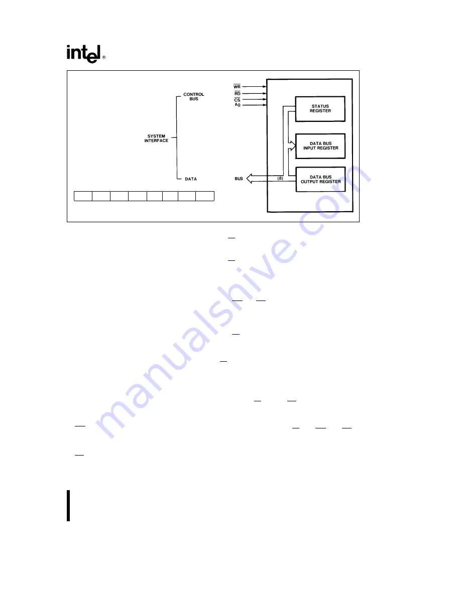
UPI Bus Contents During Status Read
ST
7
ST
6
ST
5
ST
4
F
1
F
0
IBF
0BF
D7
D6
D5
D4
D3
D2
D1
D0
231318 – 21
Figure 2-16. Data Bus Buffer Configuration
#
F
0
This is a general purpose flag which can be cleared
or toggled under UPI software control. The flag is
used to transfer UPI status information to the mas-
ter processor.
#
F
1
Command/Data
This flag is set to the condition of the A
0
input line
when the master processor writes a character to the
data register. The F
1
flag can also be cleared or tog-
gled under UPI-Microcomputer program control.
#
ST4 through ST7
These bits are user defined status bits. They are de-
fined by the MOV STS,A instruction.
SYSTEM INTERFACE
Figure 2-17 illustrates how a UPI-Microcomputer can
be connected to a standard 8080-type bus system. Data
lines D
0
– D
7
form a three-state, bidirectional port
which can be connected directly to the system data bus.
The UPI bus interface has sufficient drive capability
(400
m
A) for small systems, however, a larger system
may require buffers.
Four control signals are required to handle the data
and status information transfer:
#
WR
I/O WRITE signal used to transfer data from the
system bus to the UPI DBBIN register and set the
F
1
flag in the status register.
#
RD
I/O READ signal used to transfer data from the
DBBOUT register or status register to the system
data bus.
#
CS
CHIP SELECT signal used to enable one 8041AH
out of several connected to a common bus.
#
A
0
Address input used to select either the 8-bit status
register or DBBOUT register during an I/O READ.
Also, the signal is used to set the F
1
flag in the
status register during an I/O WRITE.
The WR and RD signals are active low and are stan-
dard MCS-80 peripheral control signals used to syn-
chronize data transfer between the system bus and pe-
ripheral devices.
The CS and A
0
signals are decoded from the address
bus of the master system. In a system with few I/O
devices a linear addressing configuration can be used
where A
0
and A
1
lines are connected directly to A
0
and
CS inputs (see Figure 2-17).
Data Read
Table 2-4 illustrates the relative timing of a DBBOUT
Read. When CS, A
0
, and RD are low, the contents of
the DBBOUT register is placed on the three-state Data
lines D
0
– D
7
and the OBF flag is cleared.
The master processor uses CS, A
0
, WR, and RD to
control data transfer between the DBBOUT register
and the master system. The following operations are
under master processor control:
21
Содержание UPI- 41A
Страница 1: ...October 1993 Microprocessor Peripherals UPI 41A 41AH 42 42AH User s Manual Order Number 231318 006 ...
Страница 4: ......
Страница 12: ...UPI 41A 41AH 42 42AH USER S MANUAL 231318 7 Figure 2 2 Pin Configuration 231318 8 Figure 2 3 Logic Symbol 8 ...
Страница 65: ...UPI 41A 41AH 42 42AH USER S MANUAL 231318 42 Figure 5 11 Distributed Processor System 61 ...


