


Hardware Design Guide
143
IXP28XX Network Processor
Slowport
.
The glue logic latches all 32 bits of read data on the rising edge of SP_CP if SP_RD_L is asserted.
The logic latches all the data on each rising edge and will always get the last 32 bits of data
presented on the data bus, and is therefore unaffected by multiple pulses of the bus. Alternately, the
rising edge of the SP_RD_L signal could be used in place of SP_CP to latch the read data; however
this procedure requires separate registers for the read and write data, as explained in
Section 7.1.2.2.4
.
The read-latching logic, shown in
Example 4
, is combined with the data-packing logic and shares
the same 32-bit register. After the data is captured, the logic must also unpack the data back to the
IXP28XX network processor at eight bits per transfer (MSB to LSB) onto the SP_AD. This is
accomplished by the glue logic driving the first byte of the read data back to the network processor
on the SP_RD_OUT bus when the signal SHIFT_EN is asserted.
Note:
The SHIFT_EN signal is used in combination with a two-bit counter, PACK_CNT, which is used to
steer the appropriate byte, based on the count, onto the SP_RD_OUT bus. The PACK_CNT
counter is incremented on every rising edge of SP_CP if the SHIFT_EN control signal is asserted;
PACK_CNT is cleared if SHIFT_EN is de-asserted. This procedure ensures that PACK_CNT will
be zero at the beginning of each read cycle. As the count increments, the appropriate byte is driven
onto the SP_RD_OUT bus as SP_CP is pulsed to complete the 32-bit transfer.
The SHIFT_EN control signal detects if the SP_OE_L signal is asserted, the SP_RD_L signal is
de-asserted, and the SP_DIR signal is de-asserted; these conditions indicate this is a read cycle and
that the glue logic owns the bus. Ultimately, the SP_RD_OUT bus connects to the output port of a
bidirectional buffer, which will connect to the SP_AD bus. The output enable for this buffer can be
controlled by SP_DIR or the SHIFT_EN control signal. The Verilog* code in
Example 5
depicts an
example implementation of the SHIFT_EN control signal and the data unpacking logic.
Note:
The SP_CP signal may pulse after the SP_RD_L signal has been deasserted; therefore, only the
SP_OE_L, SP_DIR, and SP_CP signals should be used to control the unpacking of the data.
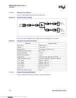
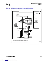
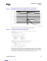
Figure 88.
Slowport Mode 3 read example showing RXE = 2
Bxxxx
CPP_CLK
1
SP_CLK
1
1
SP_DIR
SP_CP
SP_OE
SP_RD
SP_ACK
SP_ALE
SP_CS[1:0]
SP_AD[7:0]
SP_WR
1
1
1
3
1
d8
0
0
RXE = 2
Internal bus clock
Rise of SP_CP
Rise of SP_CLK
3
d8
7d
Data is latched RXE internal
clock cycles before
rising edge of SP_CLK
1
2
3
4
5
6
7
8
9
10
11
12
13
14
15
16
17
18
19
20
21
22
23
24
25
26
27
28
Downloaded from
Elcodis.com
electronic components distributor
Содержание IXP28 Series
Страница 10: ...IXP28XX Network Processor Revision History 10 Downloaded from Elcodis com electronic components distributor ...
Страница 126: ...126 Hardware Design Guide IXP28XX Network Processor PCI Downloaded from Elcodis com electronic components distributor ...
Страница 154: ...Index 154 Downloaded from Elcodis com electronic components distributor ...