•
CSEL Settings for the SD/MMC Controller
Table in the "Booting and Configuration" appendix of the Arria V Hard Processor
System Technical Reference Manual
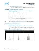
4.5.5. NAND Flash Interface Design Guidelines
GUIDELINE: Ensure that the selected NAND flash device is an 8-bit ONFI 1.0
(or later) compliant device.
The NAND flash controller in the HPS requires:
•
The external flash device to be 8-bit ONFI 1.0 compliant
•
Single-level cell (SLC) or multi-level cell (MLC)
•
Page size: 512 bytes, 2 KB, 4 KB or 8 KB
•
Pages per block: 32, 64, 128, 256, 384 or 512
•
Error correction code (ECC) sector size can be programmed to 512 bytes (for 4-,
8- or 16-bit correction) or 1024 bytes (24-bit correction)
You cannot export the NAND interface to FPGA.
Note:
Supported Flash Devices for Cyclone V and Arria V SoC
for a list of supported
NAND devices.
4.5.6. UART Interface Design Guidelines
GUIDELINE: Properly connect flow control signals when routing the UART
signals through the FPGA fabric.
When routing UART signals through the FPGA, the flow control signals are available. If
flow control is not being used, connect the FPGA signals as shown in the following
table.
Table 9.
UART Connections to Disable Flow Control
Signal
Direction
Connection
CTS
Input
Low
DSR
Input
High
DCD
Input
High
RI
Input
High
DTR
Output
No-connect
RTS
Output
No-connect
OUT1_N
Output
No-connect
OUT2_N
Output
No-connect
4. Board Design Guidelines for SoC FPGAs
AN-796 | 2018.06.18
AN 796: Cyclone V and Arria V SoC Device Design Guidelines
46

