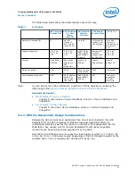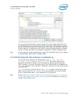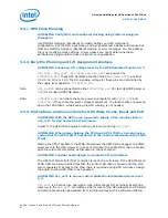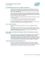
resets and reset requests from the FPGA fabric. When the HPS is internally placed in a
warm reset state, the HPS component becomes a reset source and drives the
HPS_nRST
pin low, resetting any connected board-level components.
GUIDELINE: Observe the minimum assertion time specifications of
HPS_nPOR
and
HPS_nRST
.
Reset signals on the
HPS_nPOR
and
HPS_nRST
pins must be asserted for a minimum
number of
HPS_CLK1
cycles as specified in the HPS section of the
or
.
3.3.4. Internal Clocks
GUIDELINE: Avoid cascading PLLs between the HPS and FPGA
Cascading PLLs between the FPGA and HPS has not been characterized. Unless you
perform the jitter analysis, do not chain the FPGA and HPS PLLs together as a stable
clock coming out of the last PLL in the FPGA cannot be guaranteed. Output clocks from
the HPS are not intended to be fed into PLLs in the FPGA.
3.4. HPS EMIF Design Considerations
A critical component of the HPS subsystem is the external SDRAM memory. For
Cyclone V and Arria V SoC device, the HPS has a dedicated SDRAM Subsystem that
interfaces with the HPS External Memory Interface I/O.
Review the following guidelines to properly design the interface between the memory
and the HPS. These guidelines are essential to successfully connecting external
SDRAM to the HPS.
External Memory Interface Handbook, Volume 3: Reference Material
includes the
functional description of the HPS memory controller. The supported interface options
are listed for DDR3, DDR2 and LPDDR2.
3.4.1. Considerations for Connecting HPS to SDRAM
GUIDELINE: Ensure that the HPS memory controller Data Mask (DM) pins are
enabled
In the HPS Component in Platform Designer (Standard), ensure that the checkbox to
enable the data mask pins is enabled. If this control is not enabled, data corruption
occurs any time a master accesses data in SDRAM that is smaller than the native word
size of the memory.
3. Design Guidelines for HPS portion of SoC FPGAs
AN-796 | 2018.06.18
AN 796: Cyclone V and Arria V SoC Device Design Guidelines
21


