Document Number: 002-14826 Rev. *G
Page 42 of 65
PRELIMINARY
CYW43903
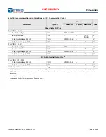
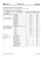
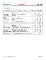
Other Digital I/O Pins
For VDDIO = 1.8V:
Input high voltage
VIH
0.65 × VDDIO
–
–
V
Input low voltage
VIL
–
–
0.35 ×
VDDIO
V
Output high voltage @ 2 mA
VOH
VDDIO – 0.45
–
–
V
Output low voltage @ 2 mA
VOL
–
–
0.45
V
For VDDIO = 3.3V:
Input high voltage
VIH
2.00
–
–
V
Input low voltage
VIL
–
–
0.80
V
Output high voltage @ 2 mA
VOH
VDDIO – 0.4
–
–
V
Output low voltage @ 2 mA
VOL
–
–
0.40
V
RF Switch Control Output Pins
4
For VDDIO_RF = 3.3V:
Output high voltage @ 2 mA
VOH
VDDIO – 0.4
–
–
V
Output low voltage @ 2 mA
VOL
–
–
0.40
V
Input capacitance
C
IN
–
–
5
pF
1. The CYW43903 is functional across this range of voltages. Optimal RF performance specified in the data sheet, however, is guaranteed only for 3V < VBAT < 4.8V.
2. VDD3P3RF, which is an internally generated supply, can drive this node. There is sufficient current and the appropriate state is maintained during hibernation and
sleep cycles.
3. Internally generated supply.
4. Programmable 2 mA to 16 mA drive strength. Default is 10 mA.
Table 16. Recommended Operating Conditions and DC Characteristics (Cont.)
Parameter
Symbol
Value
Unit
Minimum
Typical
Maximum


