background image

Document Number: 002-14826 Rev. *G 

Page 20 of 65

PRELIMINARY

CYW43903

6.  Global Functions

6.1  External Coexistence Interface

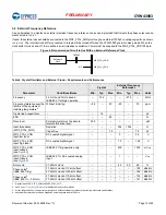
An external handshake interface is available to enable signaling between the device and an external colocated wireless device, such 
as Bluetooth, to manage wireless medium sharing for optimum performance. 

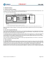
Figure 7

 shows the coexistence interface.

Figure 7. Cypress 2-Wire External Coexistence Interface

Note: 

SECI UART is the same as UART2, one of the low-speed UART interfaces mentioned in section 5.7 and in the reference 

schematics.

6.2  One-Time Programmable Memory

Various hardware configuration parameters can be stored in an internal 6144-bit (768 bytes) One-Time Programmable (OTP) memory 
that is read by system software after a device reset. In addition, customer-specific parameters, including the system vendor ID and 
MAC address can be stored, depending on the specific board design.

The initial state of all bits in an unprogrammed OTP memory device is 0. After any bit is programmed to a 1, it cannot be reprogrammed 
to 0. The entire OTP memory array can be programmed in a single write-cycle using a utility provided with the Cypress WLAN 
manufacturing test tools. Alternatively, multiple write cycles can be used to selectively program specific bytes, but only bits that are 
still in the 0 state can be altered during each programming cycle.

Prior to OTP memory programming, all values should be verified using the appropriate editable nvram.txt file. The nvram.txt file is 
provided with the reference board design package.

6.3  Hibernation Block

The Hibernation (HIB) block is a self-contained power domain that can be used to completely shut down the rest of the CYW43903. 
This optional block uses the HIB_REG_ON_OUT pin to drive the REG_ON pin. Therefore, for the HIB block to work as designed, the 
HIB_REG_ON_OUT pin must be connected to the REG_ON pin. To use the HIB block, software programs the HIB block with a wake 
count and then asserts a signal indicating that the chip should be put into hibernation. After assertion, the HIB block drives 
HIB_REG_ON_OUT low for the number of 32 kHz clock cycles programmed as the wake count. After the wake-count timer expires, 
HIB_REG_ON_OUT is driven high. Other than the logic state of the HIB block, no state is saved in the CYW43903 during hibernation.

BT\IC

GCI

WLAN

UART_IN

UART_OUT

SECI_OUT

SECI_OUT/BT_TXD and SECI_IN/BT_RXD are multiplexed on the GPIOs.

The 2‐wire coexistence interface is intended for future compatibility with the BT SIG  2‐wire interface that is being standardized for Core  4.1.

NOTES:

SECI_IN

CYW43903

Содержание Cypress WICED BCM43903

Страница 1: ...rs as part of the Infineon product portfolio Continuity of document content The fact that Infineon offers the following product as part of the Infineon product portfolio does not lead to any changes t...

Страница 2: ...ss Features Application Processor Features ARM Cortex R4 32 bit RISC processor 1 MB of on chip SRAM for code and data An on chip cryptography core 640 KB of ROM containing WICED SDK components such as...

Страница 3: ...ways On Domain UART DMA 32 KB I 32 KB D ICACHE AXI to AXI Bridge Crytography Engine APPS ARM Cortex R4 1 MB RAM 640 KB ROM SPI PWM 6 CSC GPIO 17 32 kHz External LPO PS RAM PS SR_Eng PMU Control PMU AX...

Страница 4: ...3 7 2 3 TXE 23 7 2 4 RXE 24 7 2 5 IFS 24 7 2 6 TSF 24 7 2 7 NAV 24 7 2 8 MAC PHY Interface 24 7 3 IEEE 802 11 b g n PHY 25 8 WLAN Radio Subsystem 26 8 1 Receiver Path 26 8 2 Transmit Path 26 8 3 Calib...

Страница 5: ...meters 59 18 Power Up Sequence and Timing 60 18 1 Sequencing of Reset and Regulator Control Signals 60 18 1 1 Description of Control Signals 60 18 1 2 Control Signal Timing Diagrams 60 19 Thermal Info...

Страница 6: ...embedded systems that require minimal power consumption and reliable operation Figure 2 shows the interconnect of all the major physical blocks in the CYW43903 and their associated external interfaces...

Страница 7: ...ed by reconfiguring GPIOs See Table 11 Pin Multiplexing One SPI master interface with operation up to 24 MHz Either or both of the SPI interfaces can be used as CSC master interfaces This is in additi...

Страница 8: ...WMM WMM PS U APSD WMM SA AES hardware accelerator TKIP hardware accelerator CKIP software support Proprietary Protocols CCXv2 CCXv3 CCXv4 CCXv5 WFAEC The CYW43903 supports the following additional st...

Страница 9: ...e powered down only when REG_ON is deasserted The regulators may be turned off on based on the dynamic demands of the digital baseband The CYW43903 provides a low power consumption mode whereby the CB...

Страница 10: ...B Top Always On 1 3V 1 2V 095V AVS WLRF RFPLL PFD and MMD 1 35V WLRF XTAL WLRF ADC REF WLRF TX WLRF AFE and TIA WLRF LNA WLRF LOGEN WLRF TX Mixer and PA not always 1 2V 1 2V 1 2V 1 2V 1 2V Mini PMU In...

Страница 11: ...F WL OTP 3 3V 2 5V Cap less LNLDO 2 5V Cap less LNLDO 2 5V Cap less LNLDO Inside WL Radio 3 3V VCOLDO2P5 WL RF RX TX NMOS Mini PMU LDOs WL RF VCO WL RF CP 2 5V 2 5V 450 to 800 mA Supply ball Supply bu...

Страница 12: ...timer contains 0 when the resource is enabled or disabled and a nonzero value when in a transition state The timer is loaded with the time_on or time_off value of the resource after the PMU determines...

Страница 13: ...s are disabled Input voltages must remain within the limits defined for normal operation This is done to prevent current paths or create loading on any digital signals in the system and enables the CY...

Страница 14: ...and data packet timing enabling it to operate using a wide selection of frequency references The recommended default frequency reference is a 37 4 MHz crystal The signal characteristics for the crysta...

Страница 15: ...uency 2 4 GHz and 5 GHz bands IEEE 802 11a b g n operation 37 4 37 4 MHz Frequency tolerance over the lifetime of the equipment including temperature3 3 It is the responsibility of the equipment desig...

Страница 16: ...by this wide LPO tolerance is a small current consumption increase during power save mode that is incurred by the need to wake up earlier to avoid missing beacons Whenever possible the preferred appr...

Страница 17: ...on the device attached directly to the device or accessed through a host interface The transmit pull engine reads data from the source memory and immediately passes it to the paired receive push engin...

Страница 18: ...ng In addition the JTAG interface allows Cypress to assist customers by using proprietary debug and character ization test tools during board bring up Therefore it is highly recommended to provide acc...

Страница 19: ...cle count that is programmable from 1 to 15 Programmable instructions output to serial flash An option to change the sampling edge from rising edge to falling edge for read back data when in high spee...

Страница 20: ...k cycle while the in side captures the data on or shortly after the leading edge of the clock cycle The SPI hardware block supports a hold time of 25ns and a maximum clock frequency of 40MHz If a SPI...

Страница 21: ...natively multiple write cycles can be used to selectively program specific bytes but only bits that are still in the 0 state can be altered during each programming cycle Prior to OTP memory programmin...

Страница 22: ...N is asserted Note For HIB_REG_ON_IN to function as intended HIB_REG_ON_OUT must be connected to REG_ON 2 The core LDO CLDO and LDO3P3 outputs stabilize 3 The OTP memory bits are used to initialize va...

Страница 23: ...throughput operation with low power consumption It does so without compromising the Bluetooth coexistence policies thereby enabling optimal performance over both networks In addition several power sa...

Страница 24: ...k For ALU operations the operands are obtained from shared memory scratch pad memory IHRs or instruction literals and the results are written into the shared memory scratch pad memory or IHRs There ar...

Страница 25: ...incorporates hardware that allows the MAC to enter a low power state when operating under the IEEE power save mode In this mode the MAC is in a suspended state with its clock turned off A sleep timer...

Страница 26: ...es in TX and RX TX and RX LDPC for improved range and power efficiency All scrambling encoding forward error correction and modulation in the transmit direction and inverse operations in the receive d...

Страница 27: ...d and upconverted to the 2 4 GHz ISM band Linear on chip power amplifiers deliver high output powers while meeting IEEE 802 11b g n specifications without the need for external PAs When using the inte...

Страница 28: ...O_XTAL_IN VSSC VDDIO_RF VDDIO VSSC GPIO_13 VSSC I2C0_CLK UART0_TXD VDDIO 8 7 WRF_XTAL_ XON WRF_XTAL_ GND1P2 AVSS VDDC VDDIO VDDC VSSC VSSC UART0_RXD UART0_RTS UART0_CTS 7 6 WRF_XTAL_ XOP WRF_XTAL_ VDD...

Страница 29: ...B12 SR_VDDBAT5V C1 GPIO_10 C2 GPIO_16 C3 VSSC C4 SFL_IO3 C5 SPI0_MISO C6 GPIO_12 C7 UART0_RXD C8 I2C0_CLK C9 VSSC C10 PMU_AVSS C11 VOUT_HSICLDO C12 LDO_VDD1P5 D1 GPIO_1 D2 VSSC D3 VDDC D4 VDDC D7 VSS...

Страница 30: ...H_VDD3P3 L7 VDDC L8 VSSC L9 RF_SW_CTRL_4 L10 VDDC L11 RF_SW_CTRL_1 L12 RF_SW_CTRL_7 M1 WRF_PAOUT_2G M2 WRF_TXMIX_VDD M3 WRF_AFE_GND M4 WRF_AFE_GND M5 WRF_AFE_GND M6 WRF_XTAL_VDD1P2 Ball Net Name M7 AV...

Страница 31: ...XOP I XTAL oscillator input P7 WRF_XTAL_XON O XTAL oscillator output M8 LPO_XTAL_IN I External sleep clock input 32 768 kHz H2 HIB_XTALIN I 3 3V 32 kHz crystal input J2 HIB_XTALOUT O 3 3V 32 kHz cryst...

Страница 32: ...L I JTAG select This pin must be connected to ground if the JTAG interface is not used No Connects J10 J11 J12 H9 H12 G11 N10 L4 NC_J10 NC_J11 NC_J12 NC_H9 NC_H12 NC_G11 NC_N10 WRF_EXT_TSSIA No connec...

Страница 33: ...6 I O L12 RF_SW_CTRL_7 I O M12 RF_SW_CTRL_8 I O N11 RF_SW_CTRL_9 I O SPI Flash Interface A5 SFL_CLK O Flash clock A4 SFL_IO0 I O Flash data B3 SFL_IO1 I O Flash data B4 SFL_IO2 I O Flash data C4 SFL_I...

Страница 34: ...TAL LDO input 1 35V M6 WRF_XTAL_VDD1P2 O XTAL LDO output 1 2V D11 VOUT_LNLDO O Terminate with 2 2 F capacitor to GND B11 VOUT_CLDO O Output of core LDO E12 VOUT_3P3 O LDO 3 3V output B10 VOUT_CLDO_SEN...

Страница 35: ...and Pull Up Resistances At VDDO 3 3V 10 the minimum typical and maximum weak pull down resistances for a pin voltage of VDDO are 37 99 k 44 57 k and 51 56 k respectively At VDDO 3 3V 10 the minimum ty...

Страница 36: ...CI_GPIO 0 JTAG_TCK No pull HOLD 8 mA GPIO_3 GCI_GPIO 1 JTAG_TMS No pull HOLD 8 mA GPIO_4 GCI_GPIO 2 JTAG_TDI No pull HOLD 8 mA GPIO_5 GCI_GPIO 3 JTAG_TDO No pull HOLD 8 mA GPIO_6 GCI_GPIO 4 JTAG_TRST...

Страница 37: ...XD GPIO_16 GPIO_12 TAP_SEL_P I2 C1_SDATA PWM0 GPIO_9 GPIO_9 SPI1_CLK PWM3 PWM5 UART0_TXD GPIO_0 GPIO_13 I2 C1_CLK PWM1 GPIO_10 GPIO_10 SPI1_MOSI PWM4 I2 C1_SDATA UART0_ CTS_IN PWM0 GPIO_1 GPIO_14 PWM2...

Страница 38: ...CLK GPIO_18 GPIO_25 SPI0_MOSI SPI0_MOSI GPIO_19 GPIO_26 SPI0_CS SPI0_CS GPIO_20 GPIO_27 I2 C0_SDATA I2 C0_SDATA GPIO_21 GPIO_28 I2 C0_CLK I2 C0_CLK GPIO_22 GPIO_29 1 UART_DBG_TX and UART_DBG_RX are fo...

Страница 39: ...0 I O Y Input Output PU PD or NoPull programmable Default PD Input Output PU PD or NoPull programmable Default PD High Z NoPull Input PD VDDIO GPIO_1 I O Y Input Output PU PD or NoPull programmable De...

Страница 40: ...lt NoPull High Z NoPull Input NoPull VDDIO GPIO_13 I O Y Input Output PU PD or NoPull programmable Default NoPull Input Output PU PD or NoPull programmable Default NoPull High Z NoPull Input NoPull VD...

Страница 41: ...BAT5V and LDO_VDDBAT5V supplies VBAT 0 5 to 5 5 V DC supply voltage for digital I O VDDIO 0 5 to 3 9 V DC supply voltage for RF switch I O VDDIO_RF 0 5 to 3 9 V DC input supply voltage for CLDO LNLDO...

Страница 42: ...than 60 Storage Less than 85 Operation Table 15 ESD Specifications Pin Type Symbol Condition ESD Rating Unit ESD ESD_HAND_HBM Human body model contact discharge per JEDEC EID JESD22 A114 1 5 k V CDM E...

Страница 43: ...3V Output high voltage 2 mA VOH VDDIO 0 4 V Output low voltage 2 mA VOL 0 40 V Input capacitance CIN 5 pF 1 The CYW43903 is functional across this range of voltages Optimal RF performance specified i...

Страница 44: ...GPIO_8 GPIO_9 GPIO_10 GPIO_11 GPIO_12 GPIO_13 GPIO_14 GPIO_15 GPIO_16 I2C0_CLK I2C0_SDATA I2C1_CLK I2C1_SDATA JTAG_SEL SFL_CLK SFL_CS SFL_IO0 SFL_IO1 SFL_IO2 SFL_IO3 SPI0_CLK SPI0_CS SPI0_MISO SPI0_S...

Страница 45: ...conditions specified in Table 14 Environmental Ratings and Table 16 Recom mended Operating Conditions and DC Characteristics Typical values apply for the following conditions VBAT 3 6V Ambient temper...

Страница 46: ...95 0 dBm 9 Mbps OFDM 93 8 dBm 12 Mbps OFDM 92 7 dBm 18 Mbps OFDM 90 3 dBm 24 Mbps OFDM 87 1 dBm 36 Mbps OFDM 83 6 dBm 48 Mbps OFDM 79 3 dBm 54 Mbps OFDM 78 0 dBm RX sensitivity IEEE 802 11n 10 PER fo...

Страница 47: ...48 Mbps OFDM 63 dBm 0 dB 54 Mbps OFDM 62 dBm 1 dB Adjacent channel rejection MCS0 7 Difference between interfering and desired signal 25 MHz apart at 10 PER for 4096 octet PSDU with desired signal lev...

Страница 48: ...lumn is the EVM DSS CCK 9 dB 20 5 dBm OFDM BPSK 8 dB 20 dBm OFDM QPSK 13 dB 20 dBm OFDM 16 QAM 19 dB 19 dBm OFDM 64 QAM R 3 4 25 dB 19 dBm OFDM 64 QAM MCS7 HT20 27 dB 18 5 dBm OFDM EVM2 25 C VBAT 3 6V...

Страница 49: ...us Emissions Specifications Table 22 Recommended Spectrum Analyzer Settings Parameter Setting Resolution bandwidth RBW 1 MHz Video bandwidth VBW 1 MHz Sweep Auto Span 100 MHz Detector Maximum peak Tra...

Страница 50: ...age range Programmable 30 mV steps Default 1 35V 1 2 1 35 1 5 V PWM output voltage DC accuracy Includes load and line regulation Forced PWM mode 4 4 PWM ripple voltage static Measure with 20 MHz bandw...

Страница 51: ...al output voltage Vo Default 3 3V 3 3 V Dropout voltage At max load 200 mV Output voltage DC accuracy Includes line load regulation 5 5 Quiescent current No load 85 A Line regulation Vin from Vo 0 2V...

Страница 52: ...ation Vin from Vo 0 15V to 1 5V maximum load 5 mV V Load regulation Load from 1 mA to 300 mA 0 02 0 05 mV mA Leakage current Power down 10 40 A Bypass mode 2 6 A PSRR 1 kHz Vin 1 35V Co 4 7 F 20 dB St...

Страница 53: ...from Vo 0 1V to 1 5V 150 mA load 5 mV V Load regulation Load from 1 mA to 150 mA 0 02 0 05 mV mA Leakage current Power down 10 A Output noise 30 kHz 60 150 mA load Co 2 2 F 100 kHz 60 150 mA load Co...

Страница 54: ...ad 10 12 A 55 mA load 550 570 A Line regulation Vin from Vo 0 15V to 1 5V 200 mA load 5 mV V Load regulation load from 1mA to 200 mA Vin Vo 0 15V 0 025 0 045 mV mA Leakage current Powered down Junctio...

Страница 55: ...nd all supplies are present 3 3 Sleep 4 5 4 REG_ON is high APPS domain is powered down WLAN domain is in low power state retention mode Top level is powered up 5 Inter beacon current 6 160 IEEE Power...

Страница 56: ...ding Figure 13 All Read Register commands except Read Lock Register are supported A Read Nonvolatile Configuration Register operation will output data starting from the least significant byte Figure 1...

Страница 57: ...ock Register are supported 2 The waveform must be extended for each protocol to 23 for extended and five for quad 3 A Write Nonvolatile Configuration Register operation requires data being sent starti...

Страница 58: ...4 bit addressing is used so A MAX A 23 and A MIN A 0 2 For an extended SPI protocol Cx 7 A MAX 1 3 For a quad SPI protocol Cx 1 A MAX 1 4 Figure 15 Memory Fast Read Timing 0 7 8 Cx MSB Command LSB C E...

Страница 59: ...memory write Page Program timing Note Regarding Figure 16 1 For an extended SPI protocol Cx 7 A MAX 1 2 For a quad SPI protocol Cx 1 A MAX 1 4 Figure 16 Memory Write Timing 0 7 8 Cx MSB Command LSB C...

Страница 60: ...Timing Parameters Diagram Table 31 SPI Flash Timing Parameters Parameter Description Minimum Maximum Units T_DVCH Data setup time 2 ns T_CHDX Data hold time 3 ns T_CLQX Output hold time 1 ns T_CLQV Ou...

Страница 61: ...low the regulators are disabled HIB_REG_ON_IN Used by the Hibernation HIB block to power up the internal CYW43903 regulators If the HIB_REG_ON_IN pin is low the regulators are disabled For the HIB_REG...
Страница 62: ...to account power dissipated through the top bottom and sides of the package The equation for calculating the device junction temperature is TJ TT P x YJT Where TJ Junction temperature at steady state...

Страница 63: ...Document Number 002 14826 Rev G Page 62 of 65 PRELIMINARY CYW43903 20 Mechanical Information Figure 20 WLBGA Package...

Страница 64: ...oftware from the Cypress Support Community website https community cypress com 22 3 Errata 1 The RTC block has been deprecated from this datasheet in revision A and later This block is used by Cypress...

Страница 65: ...Broadcom Serial Control BSC to Cypress Serial Control BSC throughout the document Added VBAT in Figure 1 on page 2 Updated the footnotes in Table 4 on page 14 Deleted 3 3 Frequency Selection and Real...

Страница 66: ...liability arising out of the application or use of any product or circuit described in this document Any information provided in this document including any sample design information or programming co...

Отзывы: