Document Number: 002-14826 Rev. *G
Page 40 of 65
PRELIMINARY
CYW43903
13. Electrical Characteristics
Note:
Values in this data sheet are design goals and are subject to change based on the results of device characterization.
13.1 Absolute Maximum Ratings
Caution!
The absolute maximum ratings in
indicate levels where permanent damage to the device can occur, even if these
limits are exceeded for only a brief duration. Functional operation is not guaranteed under these conditions. Operation at absolute
maximum conditions for extended periods can adversely affect long-term reliability of the device.
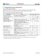
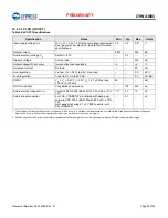
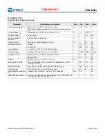
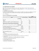
Table 13. Absolute Maximum Ratings
Parameter
Symbol
Value
Unit
DC supply for VBAT and PA driver supply
1
1. For the SR_VDDBAT5V and LDO_VDDBAT5V supplies.
VBAT
–0.5 to +5.5
V
DC supply voltage for digital I/O
VDDIO
–0.5 to 3.9
V
DC supply voltage for RF switch I/O
VDDIO_RF
–0.5 to 3.9
V
DC input supply voltage for CLDO, LNLDO, and LDO
2
2. For the LDO_VDD1P5 and WRF_XTAL_VDD1P35 supplies.
–
–0.5 to 1.575
V
3.3V DC supply voltage for RF analog
3
3. For the WRF_SYNTH_VDD3P3, WRF_PA_VDD3P3, and WRF_TXMIX_VDD supplies.
VDD3P3RF
–0.5 to 3.6
V
1.35V DC supply voltage for RF analog
4
4. For WRF_PMU_VDD1P35 and WRF_AFE_VDD1P35 supplies.
VDD1P35RF
–0.5 to 1.5
V
1.2V DC supply voltage for RF analog
5
5. For the WRF_SYNTH_VDD1P2 supply.
VDD1P2RF
–0.5 to 1.26
V
1.2V DC supply voltage for analog circuits
6
6. For the AVDD1P2 supply.
VDD1P2A
–0.5 to 1.26
V
DC supply voltage for the core
7
7. For the VDD supply.
VDDC
–0.5 to 1.32
V
DC supply voltage for OTP memory
OTP_VDD3P3
–0.5 to 3.9
V
Maximum undershoot voltage for I/O
V
undershoot
–0.5
V
Maximum junction temperature
T
j
125
°C


