Page
60 of 65
PCIe x1 Connector
( VCE-HDPCIe01 only )
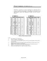
The PCIe x1 connector is a vertical, edge-finger, two-sided, 36 position
connector. Side B is on the primary ( component ) side and Side A is on
the secondary ( solder ) side. Both pins A1 and B1 are closet to the I/O
bracket.
Side B
Side A
Pin # Signal name In/Out
Note
Pin # Signal name In/Out
Note
B1
+12V
A1
PRSNT1#
O
5
B2
+12V
A2
+12V
B3
+12V
A3
+12V
B4
GND
A4
GND
B5
SMBCLK
I
1
A5
JTAG_TCK
2
B6
SMBDAT
I/O
1
A6
JTAG_TDI
2
B7
GND
A7
JTAG_TDO
2
B8
+3.3V
A8
JTAG_TMS
2
B9
JTAG_TRST#
I
2
A9
+3.3V
B10
3.3Vaux
3
A10
+3.3V
B11
WAKE#
O
2
A11
PERST#
I
6
B12
reserved
A12
GND
B13
GND
A13
I
B14
PETp0
I
7
A14
REFCLK-
I
B15
PETn0
I
7
A15
GND
B16
GND
A16
PERp0
O
7
B17
PRSNT2#
O
5
A17
PERn0
O
7
B18
GND
A18
GND
Table 7 – PCIe x1 Connector Pin-out
Notes:
1 –
The SMB Bus is not implemented.
2 –
The JTAG interface is not implemented.
3 –
3.3Vaux is used to power the WAKE# circuitry. This is a Power Management function and is
not implemented.
4 –
WAKE# is used to notify the host that it should re-apply power to the card. This is a Power
Management function and is not implemented.
5 –
PRSNT1# is tied to PRSNT2# and is used by the host to sense card insertion/removal.
6 –
PERST# is a reset signal driven by the host to reset the card.
7 –
Direction for transmit and receive signals are relative to the host.

