


Rev. 1.20
158
November 20, 2019
Rev. 1.20
159
November 20, 2019
HT66F2740
12V High Current Flash MCU
HT66F2740
12V High Current Flash MCU
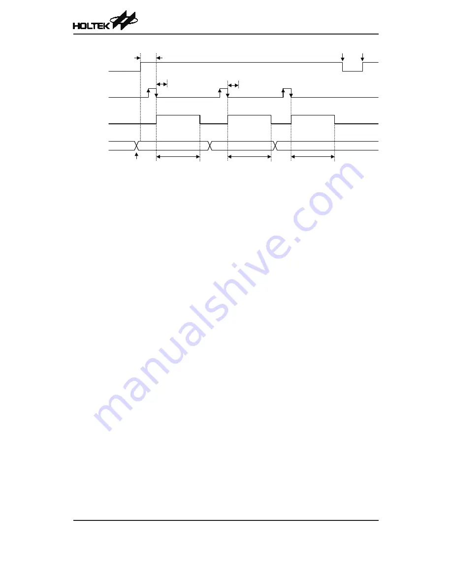
ADCEN
START
ADBZ
SACS[3:0]
(SAINS[2:0]=000)
off
on
off
on
t
ON2ST
t
ADS
A/D sampling time
t
ADS
A/D sampling time
Start of A/D conversion
Start of A/D conversion
Start of A/D conversion
End of A/D
conversion
End of A/D
conversion
t
ADC
A/D conversion time
t
ADC
A/D conversion time
t
ADC
A/D conversion time
0011B
0010B
0000B
0001B
A/D channel
switch
A/D Conversion Timing – External Channel Input
Summary of A/D Conversion Steps
The following summarises the individual steps that should be executed in order to implement an A/D
conversion process.
• Step 1
Select the required A/D conversion clock by correctly programming bits SACKS2~SACKS0 in
the SADC1 register.
• Step 2
Enable the A/D by setting the ADCEN bit in the SADC0 register to one.
• Step 3
Select which signal is to be connected to the internal A/D Converter by correctly configuring the
SAINS2~SAINS0 bits
Select the external channel input to be converted, go to Step 4.
Select the internal analog signal to be converted, go to Step 5.
• Step 4
If the A/D input signal comes from the external channel input selecting by configuring the SAINS
bit field, the corresponding pins should be configured as A/D input function by configuring the
relevant pin-shared function control bits. The desired analog channel then should be selected by
configuring the SACS bit field. After this step, go to Step 6.
• Step 5
Before the A/D input signal is selected to come from the internal analog signal by configuring the
SAINS bit field, the corresponding external input pin must be switched to a non-existed channel
input by setting the SACS3~SACS0 bits with a value from 1000 to 1111. The desired internal
analog signal then can be selected by configuring the SAINS bit field. After this step, go to Step 6.
• Step 6
Select the reference voltage source by configuring the SAVRS1~SAVRS0 bits in the SADC1
register.
• Step 7
Select A/D Converter output data format by setting the ADRFS bit in the SADC0 register.
• Step 8
If A/D conversion interrupt is used, the interrupt control registers must be correctly configured
to ensure the A/D interrupt function is active. The master interrupt control bit, EMI, and the A/D
conversion interrupt control bit, ADE, must both be set high in advance.