


Rev. 1.20
124
November 20, 2019
Rev. 1.20
125
November 20, 2019
HT66F2740
12V High Current Flash MCU
HT66F2740
12V High Current Flash MCU
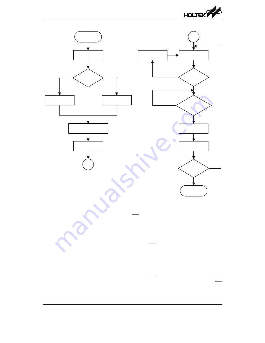
Clear WCOL
Write Data
into SIMD
WCOL=1?
Transmission
completed?
(TRF=1?)
Read Data
from SIMD
Clear TRF
END
Transfer
finished?
A
SPI Transfer
Master or Slave
?
SIMEN=1
Configure CKPOLB,
CKEG, CSEN and MLS
A
SIM[2:0]=000, 001,
010, 011 or 100
SIM[2:0]=101
Master
Slave
Y
Y
N
N
N
Y
UMD=0
SPI Transfer Control Flowchart
SPI Bus Enable/Disable
To enable the SPI bus, set CSEN=1 and SCS=0, then wait for data to be written into the SIMD
(TXRX buffer) register. For the Master Mode, after data has been written to the SIMD (TXRX
buffer) register, then transmission or reception will start automatically. When all the data has been
transferred, the TRF bit should be set. For the Slave Mode, when clock pulses are received on SCK,
data in the TXRX buffer will be shifted out and data on SDI will be shifted in.
When the SPI bus is disabled, SCK, SDI, SDO and SCS can become I/O pins or other pin-shared
functions using the corresponding pin-shared control bits.
SPI Operation Steps
All communication is carried out using the 4-line interface for either Master or Slave Mode.
The CSEN bit in the SIMC2 register controls the overall function of the SPI interface. Setting this
bit high will enable the SPI interface by allowing the SCS line to be active, which can then be used
to control the SPI interface. If the CSEN bit is low, the SPI interface will be disabled and the SCS
line will be in a floating condition and can therefore not be used for control of the SPI interface.
If the CSEN bit and the SIMEN bit in the SIMC0 are set high, this will place the SDI line in a