


Rev. 1.20
128
November 20, 2019
Rev. 1.20
129
November 20, 2019
HT66F2740
12V High Current Flash MCU
HT66F2740
12V High Current Flash MCU
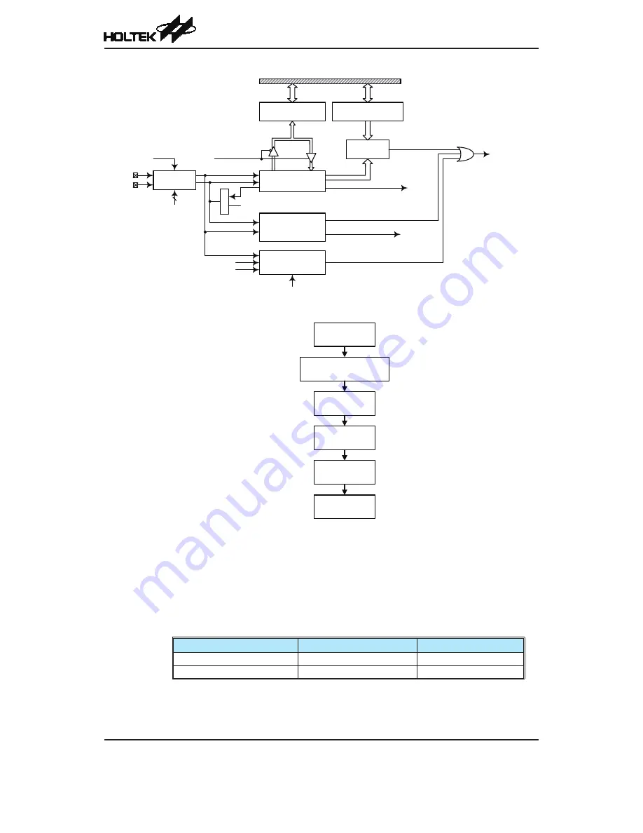
Shift Register
Transmit/
Receive
Control Unit
f
SYS
f
SUB
Data Bus
I
2
C Address Register
(SIMA)
I
2
C Data Register
(SIMD)
Address
Comparator
Read/Write Slave
SRW
Detect Start or Stop
HBB
Time-out
Control
SIMTOF
Address Match
–
HAAS
USIM Interrupt
Debounce
Circuitry
SCL Pin
M
U
X
TXAK
Data out MSB
SIMTOEN
Address Match
SIMDEB[1:0]
SDA Pin
Data in MSB
Direction Control
HTX
8-bit Data Transfer Complete
–
HCF
I
2
C Block Diagram
START signal
from Master
Send slave address
and R/W bit from Master
Acknowledge
from slave
Send data byte
from Master
Acknowledge
from slave
STOP signal
from Master
I
2
C Interface Operation
The SIMDEB1 and SIMDEB0 bits determine the debounce time of the I
2
C interface. This uses
the internal clock to in effect add a debounce time to the external clock to reduce the possibility
of glitches on the clock line causing erroneous operation. The debounce time, if selected, can be
chosen to be either 2 or 4 system clocks. To achieve the required I
2
C data transfer speed, there
exists a relationship between the system clock, f
SYS
, and the I
2
C debounce time. For either the I
2
C
Standard or Fast mode operation, users must take care of the selected system clock frequency and
the configured debounce time to match the criterion shown in the following table.
I
2
C Debounce Time Selection I
2
C Standard Mode (100kHz) I
2
C Fast Mode (400kHz)
2 system clock debounce
f
SYS
> 4MHz
f
SYS
> 10MHz
4 system clock debounce
f
SYS
> 8MHz
f
SYS
> 20MHz
I
2
C Minimum f
SYS
Frequency Requirement