background image

1-5-3

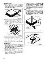
2. Installation

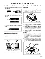
(1) Using desoldering braid, remove the solder from

the foil of each pin of the flat pack-IC on the CBA
so you can install a replacement flat pack-IC more
easily.

(2) The “

I

” mark on the flat pack-IC indicates pin 1.

(See Fig. S-1-7.) Be sure this mark matches the 1
on the PCB when positioning for installation. Then
presolder the four corners of the flat pack-IC. (See
Fig. S-1-8.)

(3) Solder all pins of the flat pack-IC. Be sure that none

of the pins have solder bridges.

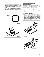
Instructions for Handling 
Semi-conductors

Electrostatic breakdown of the semi-conductors may
occur due to a potential difference caused by electro-
static charge during unpacking or repair work.

1. Ground for Human Body

Be sure to wear a grounding band (1M

) that is prop-

erly grounded to remove any static electricity that may
be charged on the body.

2. Ground for Workbench

(4) Be sure to place a conductive sheet or copper plate

with proper grounding (1M

) on the workbench or

other surface, where the semi-conductors are to be
placed. Because the static electricity charge on
clothing will not escape through the body ground-
ing band, be careful to avoid contacting semi-con-
ductors with your clothing.

Example :

Pin 1 of the Flat Pack-IC
is indicated by a "    " mark.

Fig. S-1-7

Presolder

CBA

Flat Pack-IC

Fig. S-1-8

CBA

< Incorrect >

CBA

Grounding Band

Conductive Sheet or
Copper Plate

1M

1M

< Correct >

Содержание DV-P725U

Страница 1: ...YER SPECIFICATIONS AND PARTS ARE SUBJECT TO CHANGE FOR IMPROVEMENT TK No 9205E DV P725U 2002 REV MENU TOP MENU OPEN CLOSE PHONES LEVEL PHONES MIN MAX FWD POWER STANDBY Digital Media Division Tokai April parts updated 6 12 03 ...

Страница 2: ...agram 4 1 4 DVD Main 2 4 Schematic Diagram 4 1 5 DVD Main 3 4 Schematic Diagram 4 1 6 DVD Main 4 4 Schematic Diagram 4 1 7 AV 1 3 Schematic Diagram 4 1 8 AV 2 3 Headphone Schematic Diagram 4 1 9 Waveforms 4 1 10 AV 3 3 Function Switch Schematic Diagram 4 1 11 Progressive Schematic Diagram 4 1 12 Function CBA Top View 4 1 13 Function CBA Bottom View 4 1 13 Headphone CBA Top View 4 1 13 Headphone CB...

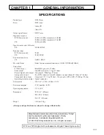
Страница 3: ...g audio output Two RCA connectors one left channel one right channel 2 Vrms 47 k ohm Component video output One pin jack Y 1 Vpp 75 ohm Two pin jacks CB PB CR PR 700mVpp 75 ohm Optical digital audio output Optical connector Power source 120 V AC 10 60 Hz 0 5 Power consumption 17 W standby 2 2W Operating temperature 5 C to 40 C Dimensions W 17 1 8 435mm H 2 15 16 75mm D 8 1 2 216mm Weight 4 63 lbs ...

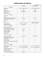
Страница 4: ...ch Shuttle Headphone Jack Volume O O Video PAL Disc NTSC Out Video Out Mode NTSC PAL PAL60 O S Video Component Composite O O O Video D A Converter 10bit Black Level Select O Picture Control Progressive Out O Audio Audio D A Converter 192kHz 24bit 96kHz 24bit Digital Audio Out Optical Coaxial O O Dolby Digital 5 1 ch Decode DTS Digital Out O Virtual Surround O Dynamic Range Compression Dolby Digita...

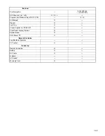
Страница 5: ...andom Play of DVD VCD O O A B Repeat O Repeat O Last Play O Closed Caption for NTSC DVD O Front Panel Display Dimmer O Screen Saver O Auto Power Off O Remote Controller Jog Shuttle on Remote TV Control O Accessory Remote Controller O Battery O AV Cable O S Cable AC Socket Warranty Card O ...

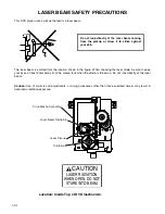
Страница 6: ...shown in the figure When checking the laser diode be sure to keep your eyes at least 30cm away from the pickup lens when the diode is turned on Do not look directly at the laser beam Caution Use of controls and adjustments or doing procedures other than those specified herein may result in hazardous radiation exposure Do not look directly at the laser beam coming from the pickup or allow it to str...

Страница 7: ...cially 1 Wires covered with PVC tubing 2 Double insulated wires 3 High voltage leads D Use specified insulating materials for hazardous live parts Note especially 1 Insulation tape 2 PVC tubing 3 Spacers 4 Insulators for transistors E When replacing AC primary side components transformers power cord etc wrap ends of wires securely about the terminals before solder ing F Observe that the wires do n...

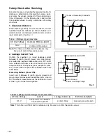
Страница 8: ...nce only Be sure to confirm the precise values 2 Leakage Current Test Confirm the specified or lower leakage current between B earth ground power cord plug prongs and externally exposed accessible parts RF termi nals antenna terminals video and audio input and output terminals microphone jacks earphone jacks etc is lower than or equal to the specified value in the table below Measuring Method Powe...

Страница 9: ...he flat pack IC with tweezers while apply ing the hot air 3 Bottom of the flat pack IC is fixed with glue to the CBA when removing entire flat pack IC first apply soldering iron to center of the flat pack IC and heat up Then remove glue will be melted Fig S 1 6 1 Release the flat pack IC from the CBA using twee zers Fig S 1 6 Caution 1 Do not supply hot air to the chip parts around the flat pack I...

Страница 10: ...s of the flat pack IC you can remove it easily Fig S 1 3 2 Affix the wire to a workbench or solid mounting point as shown in Fig S 1 5 3 While heating the pins using a fine tip soldering iron or hot air blower pull up the wire as the solder melts so as to lift the IC leads from the CBA contact pads as shown in Fig S 1 5 4 Bottom of the flat pack IC is fixed with glue to the CBA when removing entir...

Страница 11: ...e to a potential difference caused by electro static charge during unpacking or repair work 1 Ground for Human Body Be sure to wear a grounding band 1MΩ that is prop erly grounded to remove any static electricity that may be charged on the body 2 Ground for Workbench 4 Be sure to place a conductive sheet or copper plate with proper grounding 1MΩ on the workbench or other surface where the semi con...

Страница 12: ...e faster the playback speed 9 AUDIO Button Press to select a desired audio language or sound mode 10 SUBTITLE Button Press to select a desired subtitle language 11 SURROUND Button 12 PAUSE STEP Button 13 Display Remote Sensor Window 14 TV POWER Button 15 VIDEO TV Button 16 VOL Button 17 CH Button 18 FF SEARCH Button 19 SETUP Button 20 TOP MENU Button 21 DISPLAY Button 22 Numeric Buttons 23 SEARCH ...

Страница 13: ...peat function is on Stays on when the repeat function is on Lights up when a playback control is activated Displays how long a current title or track has been played back When a chapter or track has switched the number of a new title chapter or track is displayed Power on No disc inserted Tray open Tray closed Loading the Disc Power off 1 Open the battery compartment cover 2 Insert two AA batterie...

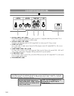
Страница 14: ...PONENT VIDEO OUT JACKS Use these jacks if you have a TV with Component Video in jacks These jacks provide CR PR CB PB and Y video Along with S Video Component Video provides the best picture quality 5 S VIDEO OUT JACK Use the S Video cable to connect this jack to the S Video jack on your A V compatible TV or wide screen TV for a higher quality picture 6 PROGRESSIVE switch DTS and DTS Digital Out a...

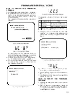
Страница 15: ... the screen and the checksum in 3 of Fig e appears on the VFD Fig f At this time no buttons are available 6 For tray opening plug the AC cord into the AC out let 7 Turn the power on by pressing the power button and the tray will close HOW TO VERIFY THE FIRMWARE VERSION 1 After making sure that no disc is in unit turn the power on 2 Press 1 2 3 4 and DISPLAY buttons on the remote control unit in th...

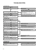
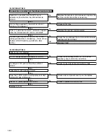
Страница 16: ...shing after 0 5 sec Are the P CON H pulse outputted from the Pin 207 of IC601 Is the P CON switch circuit operated normally Q1002 Q1005 Q1006 IC1002 D1036 D1046 Is there leaking or short circuited primary component Replace the fuse See FLOW CHART No 3 The fuse blows out Check for lead or shor circuiting of primary circuit component Q1001 Q1003 D1001 D1002 D1004 D1005 D1011 T1001 C1003 C1005 etc Ch...

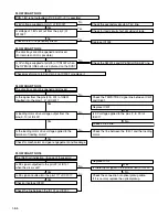
Страница 17: ...5V line Check the FL 24V line Check R2001 IC2001 and their periphery Check or replace IC2001 and IC601 Check the power circuit D1017 Q2023 Q2024 and Q2025 Check that the fluorescent display tube is free from damages such as crack FLOW CHART NO 7 The key operation is disabled Is key switch contact and installation state normal Is the control voltage normally into the pins 3 4 7 8 9 10 11 12 13 14 o...

Страница 18: ...25 of IC601 Although SEARCH 1 SEARCH PLAY STILL PAUSE STOP POWER and OPEN CLOSE button Yes Yes Is 5V voltage supplied to the pin 3 terminal of remote control receiver Yes Yes No FLOW CHART NO 9 PON 12V is not outputted Is 12V voltage supplied at collector of Q1002 Is voltage of 12V sent out from the emitter of Q1002 Check the Q1002 periphery circuit Does the P CON switch circuit operate normally Q...

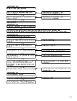
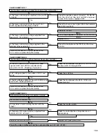
Страница 19: ...T 24V line Is voltage of 24V sent out from the anode of D1003 Check the D1003 periphery circuit Replace D1003 Check for load circuit short circuiting or leak Yes No Yes No FLOW CHART NO 12 PON 3 3V 1 2 is not outputted Is 4V voltage supplied at emitter of Q1011 Is voltage of 3 3V sent out from collector of Q1011 Check the Q1011 periphery circuit Does the P CON switch circuit operate normally Q1005...

Страница 20: ...m the pin 2 of IC1002 Check the IC1002 periphery circuit Is the signal from the pins 200 201 of IC601 inputted into the pins 1 2 of IC401 Is loading motor drive voltage output from the pins 9 10 of IC401 Is the loading motor drive voltage applied to the terminal of loading motor Check for mechanism and gear engagement and breakage Check the secondary circuit AT 5V line Check for load circuit short...

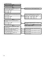
Страница 21: ...IC101 Checking of symptom Is 5V voltage applied to the emitter of Q101 and Q102 Is the 5V voltage supplied to the pin 12 DVD and pin 20 CD of pickup terminal Check the connection of optical pickup cable If it is normal replace the optical pickup Is the focus control signal outputted to the pin 115 of IC201 Is the focus control signal from the pin 115 of IC201 inputted into the pin 6 of IC401 Is th...

Страница 22: ...e peripheral circuit of JK1401 from the pin 33 of IC1402 CN701 7PIN IC1402 4PIN CVBS CN701 5PIN IC1402 6PIN S Y CN701 9PIN IC1402 2PIN S C Are the video signals shown above input into each pins of IC1402 Are the video signals outputted to each pins of IC1402 Are the video signals outputted to the specific output terminal Are the composite video signals outputted to the VIDEO OUT terminal JK1403 Ar...

Страница 23: ...and Q1204 Check the peripheral circuit of AUDIO DAC IC801 AUDIO AMP IC1201 and audio mute Q1201 Q1202 Q1203 and Q1204 circuit Check the line between each pins of main unit connector CN701 and each pins of IC1201 Check the line between each pins of main unit connector CN701 and each pins of Q1203 and Q1204 CN701 13PIN IC1201 2PIN FL CN701 15PIN IC1201 6PIN FR CN701 16PIN Q1203 Q1204 BASE AMUTE CN70...

Страница 24: ...nce Notes ID LOC No PART REMOVAL Fig No REMOVE UNHOOK UNLOCK RELEASE UNPLUG DESOLDER Note 1 Top Cover 1 5 S 1 2 Front Assembly 2 2 L 1 Tray Panel 2 L 2 CN2002 5 L 3 1 1 1 2 1 3 1 4 1 5 1 6 3 Function CBA 3 8 S 2 Jog Button Cross Button 4 DVD Mecha 4 5 3 S 3 CN101 CN401 2 2 1 2 2 2 3 3 5 Head phone CBA 4 S 4 4 L 4 CN2701 6 H P Jack Holder 4 S 5 1 Top Cover 2 Front Assembly 3 Function CBA 4 DVD Mech...

Страница 25: ...lectrostatic charge accumulated on cloth human body etc during unpacking or repair work To avoid damage of pickup follow next procedures 2 1 Slide out the pickup unit as shown in Fig 5 2 2 Short the three short lands of FPC cable with sol der before removing the FFC cable CN101 from it If you disconnect the FFC cable CN101 the laser diode of pickup will be destroyed Fig 5 2 3 Disconnect Connector ...

Страница 26: ...he three short lands by soldering View for C Slide View for A OR Short the three short lands by soldering DVD Mecha A Fig D5 10 AV CBA 9 Switch CBA 11 DVD Main CBA Unit S 11 L 6 S 9 S 10 CN1601 CN1001 S 10 S 8 Fig D6 12 Rear Panel S 12 Fig D7 ...

Страница 27: ... eject bar length approximately 80 mm diameter approximately 3 mm into the manual eject hole on the DVD Mecha Then press it until the tray is ejected Eject Bar Length approximately 80 mm Diameter approximately 3 mm Manual Eject Hole DVD Mecha Tray Top Case 1 3 2 ...

Страница 28: ...trical Parts List for parts with this mark Some Ref Numbers are not in sequence A16 2L051 2B2 A17 AC1001 2L031 2L101 2L101 2L103 2B20 2B22 2B23 2B21 2B24 W1602 Switch CBA JK1201 IC1204 JK1403 JK1401 2B4 AV CBA 003 W2201 Progressive CBA Unit 002 2L023 2L023 2B19 2L102 2L103 Headphone CBA Function CBA 004 A1X A7 2B16 A8 A19 A2 DVD Main CBA Unit 001 ...

Страница 29: ... CORD 1B1 TS17001 DVD MECHA 2B2 TJ15681 POWER PCB HOLDER 2B4 TJ15651 EARTH PLATE 2B16 TJ15486 JOG RING 2B19 TJ15487 H P JACK HOLDER 2B20 TJ15488 PRS PCB HOLDER 2L021 TJ15682 SCREW M3X10 2L023 TJ15683 SCREW M3X6 2L031 TJ15683 SCREW M3X6 2L051 TJ15682 SCREW M3X10 2L101 TJ15683 SCREW M3X6 2L102 TJ15683 SCREW M3X6 2L103 TJ10177 SCREW 3X8 001 TS17171 DVD MAIN CBA UNIT 002 TS17181 PROGRESSIVE CBA 003 TS...

Страница 30: ...Q018EF01SZ IC1003 TC12241 IC KIA431 AT IC1006 TC12241 IC KIA431 AT IC1201 TC12251 IC KIA4558P IC1204 TC12261 TRANS MODULE 0C 0805T 002 IC1402 TC12271 IC MM1567AJ IC2001 TC12281 IC PT6315 S IC2701 TC12431 IC BH3544F E2 SYMBOL NO P NO DESCRIPTION Q1001 TC12291 TRANSISTOR 2SK3374 Q1002 TC10778 TRANSISTOR KTC3199 GR Q1003 TC10778 TRANSISTOR KTC3199 GR Q1004 TC12301 TRANSISTOR KTC3205 Y Q1005 TC12311 T...

Страница 31: ... TACT SWITCH SW2208 TE11957 TACT SWITCH SW2209 TE11957 TACT SWITCH SW2210 TE11957 TACT SWITCH W1001 TE14841 CABLE 26P W1601 TE14851 CABLE 18P W1602 TE14971 CABLE 12P W1801 TE14961 CABLE 18P W2201 TE14861 CABLE 12P W2701 TE14991 CABLE 4P WJ1003 TE14871 WIRE WJ1004 TE14881 WIRE SYMBOL NO P NO DESCRIPTION SYMBOL NO P NO DESCRIPTION ...

Страница 32: ...r voltage wattage etc Replacement parts that have these special safety char acteristics are identified in this manual and its supple ments electrical components having such fea tures are identified by the mark in the schematic diagram and the parts list Before replacing any of these compo nents read the parts list in this manual carefully The use of substitute replacement parts that do not have th...

Страница 33: ...iginal function and reliability of repaired units use only original replacement parts which are listed with their part numbers in the parts list section of the service manual 4 Wire Connectors 1 Prefix symbol CN means connector can disconnect and reconnect 2 Prefix symbol CL means wire solder holes of the PCB wire is soldered directly 5 Mode SP 6 Voltage indications for PLAY mode on the schematics...

Страница 34: ... CN1601 W1601 JP1003 JP1004 AC CORD AUDIO OUT L AUDIO OUT R VIDEO OUT DIGITAL AUDIO OUT S VIDEO OUT OPTICAL AUDIO OUT EV 2 5V 3 3 25 25 26 26 NU REMOTE CN3001 SW CBA M M SPINDLE MOTOR SLIDE MOTOR RELAY CBA 19 20 21 GND CD PD CD LD CD DVD 1 2 3 4 5 6 7 8 9 10 11 DETECTOR FS TS VIDEO Y OUT HEADPHONE JACK VIDEO U OUT VIDEO V OUT SPDIF 18 18 AUDIO L 13 13 KEY 5 1 1 KEY 6 2 2 GND 3 3 KEY 7 4 4 K1 5 5 N...

Страница 35: ...4 1 4 DVD Main 1 4 Schematic Diagram ...

Страница 36: ...4 1 5 DVD Main 2 4 Schematic Diagram ...

Страница 37: ...4 1 6 DVD Main 3 4 Schematic Diagram ...

Страница 38: ...4 1 7 DVD Main 4 4 Schematic Diagram ...

Страница 39: ...cuit are not defective before you connect the AC plug to the AC power supply Otherwise it may cause some components in the power supply circuit to fail CAUTION FOR CONTINUED PROTECTION AGAINST FIRE HAZARD REPLACE ONLY WITH THE SAME TYPE FUSE ATTENTION POUR UNE PROTECTION CONTINUE LES RISQES D INCELE N UTILISER QUE DES FUSIBLE DE MEMO TYPE RISK OF FIRE REPLACE FUSE AS MARKED This symbol means fast ...

Страница 40: ...4 1 9 AV 2 3 Headphone Schematic Diagram ...

Страница 41: ...DE WF1 WF3 WF6 SPDIF Pin 18 of CN1601 1V 0 2usec WF1 Pin 5 of CN1601 WF3 Pin 9 of CN1601 WF4 AUDIO L Pin 13 of CN1601 1V 0 5msec WF5 AUDIO R Pin 15 of CN1601 1V 0 5msec WF2 Pin 7 of CN1601 VIDEO Y 0 2V 20usec VIDEO CVBS 0 5V 20usec VIDEO C 0 2V 20usec WAVEFORM ...

Страница 42: ...4G 6G 2G a d g c b e f 1 3 2 4 5 DVD VCD PBC STANDBY A B REPEAT TRK CHP TITLE 7G 6G 5G 4G 3G 2G 1G a b c d e f g c d e f g c d e f g c d e f g c d e f g c d e f g h i a b a b a b a b a b FL2001 MATRIX CHART STANDBY TITLE CHP TRK CD V PBC DVD REPEAT A B 1 3 2 4 5 ...

Страница 43: ...4 1 12 Progressive Schematic Diagram ...

Страница 44: ...4 1 13 Function CBA Top View Function CBA Bottom View Headphone CBA Top View Headphone CBA Bottom View ...

Страница 45: ...POWER SUPPLY CIRCUIT AN ISOLATION TRANSFORMER MUST BE USED ALSO IN ORDER TO HAVE THE ABILITY TO INCREASE THE INPUT SLOWLY WHEN TROUBLESHOOTING THIS TYPE POWER SUPPLY CIRCUIT A VARIABLE ISOLATION TRANSFORMER IS REQUIRED CAUTION FOR CONTINUED PROTECTION AGAINST FIRE HAZARD REPLACE ONLY WITH THE SAME TYPE FUSE ATTENTION POUR UNE PROTECTION CONTINUE LES RISQES D INCELE N UTILISER QUE DES FUSIBLE DE ME...

Страница 46: ...t to fail BECAUSE A HOT CHASSIS GROUND IS PRESENT IN THE POWER SUPPLY CIRCUIT AN ISOLATION TRANSFORMER MUST BE USED ALSO IN ORDER TO HAVE THE ABILITY TO INCREASE THE INPUT SLOWLY WHEN TROUBLESHOOTING THIS TYPE POWER SUPPLY CIRCUIT A VARIABLE ISOLATION TRANSFORMER IS REQUIRED CAUTION FOR CONTINUED PROTECTION AGAINST FIRE HAZARD REPLACE ONLY WITH THE SAME TYPE FUSE ATTENTION POUR UNE PROTECTION CONT...

Страница 47: ...GMENT KEY MATRIX SHUTTLE FL2001 IC2001 DVD MAIN CBA UNIT AV CBA SWITCH CBA FUNCTION CBA FG CBA RELAY CBA FRONT PANEL CONTROL BLOCK DIAGRAMS TREV TIN TOUT TFWD MUTE PS CD DVD CFE CAS STANDBY ADDRESS BUS DATA BUS CD DVD CFE CAS STANDBY 71 62 63 70 SCK 72 STDIO SEN SCK STDIO 13 14 16 3 4 FG SENSOR CN401 FP STB 21 21 FP DIN 22 22 FP DOUT 23 23 FP CLK 24 24 REMOTE 26 26 207 PWRCON PWRCON 20 20 CN2201 S...

Страница 48: ...Q102 AMP FOCUS MOTOR DRIVE TRACKING MOTOR DRIVE LOADING MOTOR DRIVE SPINDLE MOTOR DRIVE POWER SAVE SLIDE MOTOR DRIVE LOADING MOTOR SPINDLE MOTOR SLIDE MOTOR M 5 21 2 1 23 26 25 27 22 24 4 67 115 114 118 117 DVD MAIN CBA UNIT FROM TO SYSTEM CONTROL BLOCK DIAGRAM FROM TO DVD SIGNAL PROCESS BLOCK DIAGRAM SCK CD DVD TESTSG ARF NARF STDIO SEN 11 STANDBY TRAY IN 3 GND 5 TRAY OUT 4 TRAY IN TRAY OUT DAC1 ...

Страница 49: ...R PLL VCO CPU INTERFACE VIDEO AUDIO INTERFACE DVD DEMODULATOR MEMORY MANAGER 172 168 166 164 160 158 151 149 82 TO VIDEO BLOCK DIAGRAM BCA DATA VIDEO AUDIO SIGNAL DVD MAIN CBA UNIT FROM TO SYSTEM CONTROL BLOCK DIAGRAM CPUDT0 NINT1 ADDRESS BUS DATA BUS NINT2 NINT1 NINT2 WAIT RE WEL CS1 RESET WAIT RE WEL CS1 RESET CPUDT7 30 22 17 9 44 37 CPUADR0 CPUADR17 2 5 6 36 35 34 47 OSCI1 X201 16 9344MHz OSCO1...

Страница 50: ... ST20 ARBITER MEMORY CONTROLLER SDRAM ARBITER SHARED SDRAM INTERFACE I F VIDEO DECODER AUDIO DECODER CACHE SUBSYSTEM CPU VIDEO FILTERING OSD SP DECODER MIXING 4dB AMP 2dB AMP LPF DRIVER Y C CD FIFO SDRAM BLOCK MOVE DENC SPDIF PCM LRCLK PCM SCLK PCM DATA0 PCM BCK FROM DVD SIGNAL PROCESS BLOCK DIAGRAM TO AUDIO BLOCK DIAGRAM DVD MAIN CBA UNIT 48 2 33 97 102 84 93 4dB AMP 2dB AMP LPF DRIVER VIDEO V OU...

Страница 51: ...YNC CLOCK RESET SDA SCL 136 125 ADDR0 ADDR10 139 176 DATA0 DATA31 IC1806 1 3 2 F F IC1807 1 4 2 IC1808 20 24 27 32 ADDR0 RAM F F AND GATE RAM 5V SW1801 MUTE ADDR10 2 12 39 49 DATA0 DATA15 IC1809 20 24 27 32 ADDR0 ADDR10 2 12 39 49 DATA16 DATA31 DRIVE CN1802 IC1802 34 36 6dB DR 10 6dB DR 15 6dB DR 4 2 2 TO 4 4 4 4 2 2 TO 4 4 4 DATA VIDEO SIGNAL VIDEO SIGNAL Progressive Block Diagram FROM TO VIDEO B...

Страница 52: ...EO BLOCK DIAGRAM SERIAL PORT SERIAL CONTROL 4X 8X OVERSAMPLING DIGITAL FILTER FUNCTION CONTROLLER ENPHANCED MULTI LEVEL DELTA SIGMA MODULATOR DAC LPF AMP L CH R CH LPF AMP DAC ZERO DETECT SYSTEM CLOCK 1 2 6 7 5 AUDIO R OUT CN2701 HPR HPL PCM BCK SPDIF PCM DATA0 PCM LRCLK ADAC MD ADAC MC ADAC ML PCM SCLK AV CBA HEADPHONE CBA DVD MAIN CBA UNIT AUDIO SIGNAL DATA AUDIO SIGNAL 18 18 SPDIF A MUTE 3 3V Q...

Страница 53: ... P ON 12V EV 5V IC1006 SHUNT REGULATOR SWITCHING D1008 D1030 RECTIFIER D1003 RECTIFIER D1009 RECTIFIER D1013 D1016 RECTIFIER SWITCHING CONTROL LATCH REG 1 2 6 BRIDGE RECTIFIER HOT AV CBA REPLACE FUSE AS MARKED Ce symbole reprèsente un fusible à fusion rapide CAUTION FOR CONTINUED PROTECTION AGAINST FIRE HAZARD REPLACE ONLY WITH THE SAME TYPE FUSE ATTENTION POUR UNE PROTECTION CONTINUE LES RISQES D...

Страница 54: ... LM I o TL123 SP TP122 Tv TL122 0V 5V 0V Tray close Tray open Tray close Play Play Tray open Play 0V Eject key on 6V 2V 5V 0V Disc Rotation Eject key on 2V 2 0s 0V 6V 4 4s 1 2s 700ms 1 7s 0V SYSTEM CONTROL TIMING CHARTS ...

Страница 55: ...put Key Source 2 9 Out c Key 3 Segment Output Key Source 3 10 Out d Key 4 Segment Output Key Source 4 11 Out e Key 5 Segment Output Key Source 5 12 Out f Key 6 Segment Output Key Source 6 13 Out g Key 7 Segment Output Key Source 7 14 Out h Key 8 Segment Output Key Source 8 15 VEE Pull Down Level 16 Out i Segment Output 17 Out 7G Grid Output 18 6G 19 5G 20 4G 21 3G 22 2G 23 1G 24 VDD Power Supply 2...

Страница 56: ...28 15 14 PT6315 S PT6315 S TP 1 34 18 17 MM1567AJ 1 E C B 2SA1015 Y TPE2 KTA1266 Y 2SC2236 Y TPE6 C E C B 2SC2785 H KTC3199 GR KRA110M KRC110M AT BA1L3Z T BA1L3Z P KTC3205 Y A K C E LTV 817B F LTV 817C F R A K KIA431 AT AN1431 NSC 1 4 PQ018EF01SZ 0C 0805T 002 GP1FA512TZV G D S 2SK3374 1 2 3 E C B 2SC3422 LEAD IDENTIFICATIONS ...

Страница 57: ...DV P725U DV P725U DV P725U No 9205E TK Digital Media Division Tokai ...

Отзывы: