DP-4X SIGNAL POWER SUPPLY 5.7V REGULATION EXPLANATION
PAGE 01-1
9
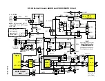
5.7V Power Supply Regulation Circuit Diagram explanation:
(See Signal Power Supply 5.7V Regulation Circuit Diagram for details)
THIS POWER SUPPLY RUNS ONLY WHEN THE POWER 1 COMMAND IS ACTIVE HIGH:
TURNING ON THE 5.7V POWER SUPPLY:
(
See Power On/Off Circuit Diagram).
RY101
directs AC to the Low Voltage Power Supply.
When the set is turned on, the
POWER SIG
command is supplied from pin
59
of the Microprocessor
I004
. This
high is sent to
Q018
and
Q021
then to the
PPS1
connector pin
9
labeled
POWER 1
. From here this high goes
through
R110
and then
D109
to the Base of
Q101
. The base goes high and the transistor turns on. This action
supplies a ground return for the coil inside
RY101
and the relay turns on supplying AC through
F102
to the Sig-
nal Power Supply rectifier
DS201
and the Signal Power Supply begins to operate.
DS201
develops raw 150V which is routed through
T201
primary to the Drain of
Q201
. From the Source of
Q201
(when switched) the primary of
T201
is grounded through a 0.1 low ohm resistors
R204
.
As the current draw across
R204
rises and falls due to the load, the developed DC Voltage is sent to pin
3
of
IC201
which is the Over Current Detection pin. If this voltage goes too high, the power supply will shut down
until the over
voltage condition disappears.
Q201
gate control is via pin
5
of
IC201
.
After the Signal Power Supply begins to operate,
IC201
needs
Run Voltage
. This is accomplished by the pulse
from
T201
which is rectified by
D204
, filtered by
C206
and the DC component arrives at pin
6
of
IC201
.
5.7V REGULATION
5.7V pulse is generated from on the secondary of
T201
. This pulse is rectified by
D210
, filtered by
C228
and
C229
.
The primary route for the
5.7V
is through
L204
and output as
DM 5.6V
to the Digital Module.
However, the regulation route is to the cathode of
IC203
. This regulator circuit works as a variable resistor
whose resistance is dependant upon the
5.7V
voltage fluctuations. This variable resistor manipulates the current
flow from pin
2
of
PC201
. Internally, the LED is illuminated by degrees dependant upon the
5.7V
voltage fluc-
tuations which causes the resistance of
IC203
to fluc
t
uate. The internal receiver receives this light and acts as a
variable resistor from pin
4
to pin
3
,
which is the regulation control signal to pin
2
labeled as
F/B
.
This action causes pin
2
of
IC201
to manipulate the internal oscillator within
IC201
. This in turn causes the tim-
ing of the drive pulses delivered to the Gate of
Q201
SMOSFET (Switch Metal Oxide Semiconductor Field Ef-
fect Transistor) to manipulate the frequency of the pulse generated on the primary of
T201
. The current drain of
these SMOSFETs is monitored by the low ohm resistor
R204
mentioned above. If this current exceeds a specific
value, the voltage developed by this low ohm resistor is routed through
R213
back into pin
3
of
IC201
which is
the Over Current Protection circuit. This pin will inhibit the drive signal to the gate of the SMOSFETs. As soon
as the excessive current situation is eliminated, the IC will recover and continue functioning.
B+ GENERATION FOR THE POWER SUPPLY DRIVER IC201:
Vcc for the Driver IC is first generated by the AC input. This voltage is called
Start Up Voltage
.
IC201
requires
23.3V
DC to operate normal. However, it will begin operation at a much smaller voltage on pin
6
.
When AC is applied to the main full wave bridge rectifier
DS201
where it is converted to Raw 150V DC voltage,
filtered by
C201
and
C202
, routed through
R202
,
R203
and
R210
and made available to pin
6
of
IC201
as start
up voltage. When this voltage reaches 12Vdc, the internal Regulator of
IC201
is turned On and begins operation.
When the power supply begins to operate, the magnet field collapses and the EMF is coupled over to the secon-
dary windings, as well as the drive windings. One drive winding produces a run voltage pulse which is rectified
by
D204
, filtered by
C206
and becomes run voltage (
23.3V
) for
IC201
pin
6
.
Содержание 51F510
Страница 2: ...DP 4X BLANK PAGE NOTES BLANK PAGE ...
Страница 5: ...DP 4X CHASSIS INFORMATION POWER SUPPLY INFORMATION SECTION 1 ...
Страница 6: ...DP 4X BLANK PAGE NOTES BLANK PAGE ...
Страница 30: ...DP 4X BLANK PAGE NOTES BLANK PAGE ...
Страница 31: ...DP 4X CHASSIS INFORMATION MICROPROCESSOR INFORMATION SECTION 2 ...
Страница 32: ...DP 4X BLANK PAGE NOTES BLANK PAGE ...
Страница 44: ...DP 4X BLANK PAGE NOTES BLANK PAGE ...
Страница 45: ...DP 4X CHASSIS INFORMATION VIDEO INFORMATION SECTION 3 ...
Страница 46: ...DP 4X BLANK PAGE NOTES BLANK PAGE ...
Страница 61: ...DP 4X CHASSIS INFORMATION AUDIO INFORMATION SECTION 4 ...
Страница 62: ...DP 4X BLANK PAGE NOTES BLANK PAGE ...
Страница 66: ...DP 4X BLANK PAGE NOTES BLANK PAGE ...
Страница 67: ...DP 4X CHASSIS INFORMATION DEFLECTION INFORMATION SECTION 5 ...
Страница 68: ...DP 4X BLANK PAGE NOTES BLANK PAGE ...
Страница 79: ...DP 4X CHASSIS INFORMATION DIGITAL CONVERGENCE INFORMATION SECTION 6 ...
Страница 80: ...DP 4X BLANK PAGE NOTES BLANK PAGE ...
Страница 94: ...DP 4X BLANK PAGE NOTES BLANK PAGE ...
Страница 95: ...DP 4X CHASSIS INFORMATION CHASSIS PICTURES SECTION 07 ...
Страница 96: ...DP 4X BLANK PAGE NOTES BLANK PAGE ...
Страница 104: ...DP 4X BLANK PAGE NOTES BLANK PAGE ...
Страница 105: ...DP 4X CHASSIS INFORMATION DP 4X CHASSIS ADJUSTMENTS SECTION 08 ...
Страница 106: ...DP 4X BLANK PAGE NOTES BLANK PAGE ...
Страница 108: ...DP 4X BLANK PAGE NOTES BLANK PAGE ...
Страница 144: ...DP 4X BLANK PAGE NOTES BLANK PAGE ...
Страница 146: ...DP 4X BLANK PAGE NOTES BLANK PAGE ...
Страница 147: ...DP 4X CHASSIS INFORMATION SERVICE POLICY FOR THE DP 4X CHASSIS SECTION 10 ...
Страница 148: ...DP 4X BLANK PAGE NOTES BLANK PAGE ...
Страница 151: ...DP 4X BLANK PAGE NOTES BLANK PAGE ...
Страница 152: ...DP 4X BLANK PAGE NOTES BLANK PAGE ...


