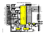

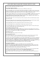
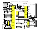


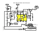

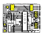

DP-3X SWEEP LOSS DETECTION CIRCUIT EXPLANATION
PAGE 05-05
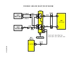
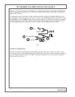
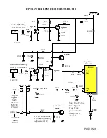
(See Sweep Loss Detection Circuit for details)
The key component in the Sweep Loss Detection circuit is
QN02
. This transistor is normally biased off by the
pull up resistor
RN18
. When the base becomes 0.6V below the emitter, it will be turned on, causing the SW
+10V to be applied to two different circuits, the Spot circuit and the High Voltage Drive circuit. Either
QN03
or
QN04
turning on, will turn
QN02
on.
SPOT ACTIVATION CIRCUIT
When
QN02
is turned on, the SW +10V will be applied to the anode of
DN11
, forward biasing it. This voltage
will then pass through
DN11
. It will then be clamped by
DN12
, and arrive at pin
4
of
PPD3, PPS3
. It will then
be directed to the Signal PWB where it will pass through
D511
and activate the Video Mute circuitry
Q529 -
Q527
. This is done to prevent CRT burns.
(See Audio Video Mute Circuit for details)
A control (enable) circuit for SPOT is routed from pin
5
of
PPS3, PPD3
called
“
CUT OFF
”. This will activate
when accessing certain adjustments parameters in the service mode; i.e. turning off vertical drive for making
CRT drive or cut-off adjustments. When Vertical Drive is defeated, the Vertical Sweep loss circuit would acti-
vate. Cut Off is produced from the Microprocessor
I001
pin
47
and routed to
QN06
to “inhibit” the Spot line
from activating and shutting off the CRTs.
HIGH VOLTAGE DRIVE CIRCUIT
When
QN02
is turned on, the SW +10V will also be routed through
RN15
and
DN09
and applied to the High
Voltage Drive IC
IH01
at pin
14
. When this occurs, the IC will stop generating the drive signal from pin
1
that is
used to produce High Voltage via
QH02
, the High Voltage Driver. Again, this is done to prevent CRT burn, es-
pecially during sweep loss.
This high is also routed through
RN16
,
DN10
to pin
3
of
IH01
which also kills the internal drive.
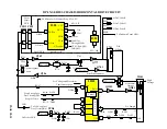
CONCERNING QN02
There are several factors that can cause
QN02
to activate; loss of vertical or horizontal blanking.
Loss of Vertical Blanking (V Blk)
The Vertical pulse at the base of
QN05
switches
ON05
on and off at the vertical rate. This discharges
CN03
suf-
ficiently enough to prevent the base of
QN04
from going high to turn it on and activate
QN02
.
When the 24 Vp/p positive vertical blanking pulse is missing from
CN04
to the base of
QN05
, it will be turned
off, which will cause the collector to pull up high because
CN03
charges up through
RN11
. This in turn will
cause
QN04
to turn on because it’s base pulls up high, creating an increase of current flow from emitter to collec-
tor and through
RN09. RN08
, (which is located across the emitter base junction of
QN02
), to the SW +10V sup-
ply. This increase of current flow through
RN08
will bias on
QN02
and the events described in “Spot Activation
Circuit” above will occur.
Loss of Horizontal Blanking (H Blk)
The Horizontal pulse at the base of
QN01
switches
ON01
on and off at the horizontal rate. This discharges
CN02
sufficiently enough to prevent the base of
QN03
from going high to turn it on and activate
QN02
.
When the 11.6 Vp/p positive horizontal blanking pulse is missing from
CN01
to the base of
QN01
, it will be
turned off, which will cause the collector to go high through
DN03
,
RN02
as the SW +10V charges
CN02
. This
in turn will cause
QN03
to turn on because it’s base is pulled up high when
DN02
fires. When
QN03
turns on, an
increase of current flow from emitter to collector, through
RN10
, and up through
RN08
. This increase of current
flow through
RN08
will bias on
QN02
and the events described in “Spot Activation Circuit” above will occur.
Содержание 46W500
Страница 2: ...DP 3X BLANK PAGE NOTES BLANK PAGE ...
Страница 6: ...DP 3X BLANK PAGE NOTES BLANK PAGE ...
Страница 7: ...DP 3X CHASSIS INFORMATION POWER SUPPLY INFORMATION SECTION 1 ...
Страница 8: ...DP 3X BLANK PAGE NOTES BLANK PAGE ...
Страница 23: ...DP 3X CHASSIS INFORMATION MICROPROCESSOR INFORMATION SECTION 2 ...
Страница 24: ...DP 3X BLANK PAGE NOTES BLANK PAGE ...
Страница 35: ...DP 3X CHASSIS INFORMATION VIDEO INFORMATION SECTION 3 ...
Страница 36: ...DP 3X BLANK PAGE NOTES BLANK PAGE ...
Страница 50: ...DP 3X BLANK PAGE NOTES BLANK PAGE ...
Страница 51: ...DP 3X CHASSIS INFORMATION AUDIO INFORMATION SECTION 4 ...
Страница 52: ...DP 3X BLANK PAGE NOTES BLANK PAGE ...
Страница 57: ...DP 3X CHASSIS INFORMATION DEFLECTION INFORMATION SECTION 5 ...
Страница 58: ...DP 3X BLANK PAGE NOTES BLANK PAGE ...
Страница 69: ...DP 3X CHASSIS INFORMATION DIGITAL CONVERGENCE INFORMATION SECTION 6 ...
Страница 70: ...DP 3X BLANK PAGE NOTES BLANK PAGE ...
Страница 83: ...DP 3X CHASSIS INFORMATION ADJUSTMENT INFORMATION SECTION 7 ...
Страница 84: ...DP 3X BLANK PAGE NOTES BLANK PAGE ...
Страница 98: ...DP 3X BLANK PAGE NOTES BLANK PAGE ...
Страница 99: ...DP 3X CHASSIS INFORMATION MISCELLANEOUS INFORMATION SECTION 8 ...
Страница 100: ...DP 3X BLANK PAGE NOTES BLANK PAGE ...
Страница 111: ...DP 3X CHASSIS INFORMATION DP 33W 46W500 DVD PLAYER TROUBLESHOOTING SECTION 9 ...
Страница 112: ...DP 3X BLANK PAGE NOTES BLANK PAGE ...
Страница 131: ...DP 3X CHASSIS INFORMATION THINGS YOU SHOULD KNOW SECTION 10 ...
Страница 132: ...DP 3X BLANK PAGE NOTES BLANK PAGE ...
Страница 134: ...DP 3X BLANK PAGE NOTES BLANK PAGE ...
Страница 161: ...DP 3X BLANK PAGE NOTES BLANK PAGE ...
Страница 162: ...DP 3X BLANK PAGE NOTES BLANK PAGE ...


