


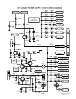


DP-3X POWER SUPPLY SHUT DOWN EXPLANATION
PAGE 01-06
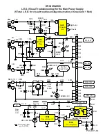
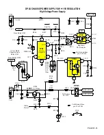
B+ GENERATION FOR THE MAIN POWER SUPPLY DRIVER IC I901:
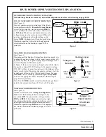
Vcc for the Driver IC is first generated by the AC input. This voltage is called Start Up Voltage.
I901
normal pin
4
voltage is
23.3V
. However, it will begin operation at
12V
on pin (
4
) of
I901
. When the set is turned on by
S901
, AC is applied. AC is
routed through the main fuse
F901
(a 10 Amp fuse),
then through the Line filter
L901
to prevent any internal high frequency
radiation for radiating back into the AC power line. After passing
L901
filter it passes another filter
L903
. The HOT leg of
AC is routed through the relay
S901
and AC arrives at the main full wave bridge rectifier
D901
where it is converted to Raw
150V DC voltage to be supplied to the power supply switching transformer
T901
pins (
1
and
2
).
However, one leg of the AC is routed to
R906
and
R907
(both a 3.9K ohm resistor), filtered by
C911
, clamped by a 36V
Zener
D911
and made available to pin (
4
) of
I901
as start up voltage. When this voltage reaches 13Vdc, the internal Regula-
tor of
I901
is turned On and it begins to operate.
When the power supply begins to operate by turning on and off the internal Switch MOS FET, the Raw 150V DC routed
through
T901
, in on pin
3
(Drain) and out on pin
2
which is the Source. The Source of the internal Switch MOS FET is routed
out of pin (
2
) through four low ohm resistors (
R908, R909, R910 and R911
) to hot ground. When the internal Switch MOS
FET turns on, it causes the transformer to saturate building up the magnet field. When the internal Switch MOS FET turns off,
the magnet field collapses and the EMF is coupled over to the secondary windings, as well as the drive windings. The drive
windings at pin (
8
) produce a run voltage pulse which is rectified by
D907
, filtered by
C911
then routed clamped by
D911
and now becomes run voltage (
23.3V
) for
I901
pin
4
.
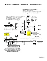
HOT GROUND SIDE SHUT DOWN SENSING CIRCUITS. (Specific to I901).
In addition, there are 4 Hot Ground side Shutdown inputs that are specifically detected by the main power driver IC
I901
.
These sensors circuits protect
I901
from excessive current, temperature or over voltage.
LATCHED SHUT DOWN MONITORS:
(AC must be removed to recover).
1.
(OVP)
Pin 4
is monitored for Over Voltage Protection at pin
4
of
I901
.
2.
(TSD)
I901
itself is monitored for Excessive Heat. This block is labeled TSD. (Thermal Sensing Device).
3.
(Trigger) Over Load Protection monitors the difference between the Hot Ground and Floating Ground.
RECOVERING SHUT DOWN INPUT:
(Driver IC will recover on it’s own when trouble is removed.)
4.
(OCP)
Pin 1
monitors the low ohm resistors,
R908, R909, R910
and
R911
. If these resistors have an excessive current
condition caused by monitoring the current through the internal Switch MOS FET, the voltage will rise and pin
1
has an
internal Over Voltage detection op-amp. If this voltage rises enough to trigger this op-amp, the IC will stop producing a
drive signal.
(Continued on page 7)
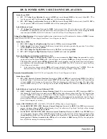
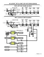
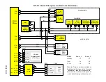
Any Positive
B+ Supply
B+
Q1
Shut-Down Signal
Voltage
Loss
Detector
Figure 4
VOLTAGE LOSS or SHORT DETECTION
(
See Figure 4)
One circuit used is the
Voltage Loss Detection
cir-
cuit. This is a very simple circuit that detects a loss
of a particular power supply and supplies a Pull-
Down path for the base of a PNP transistor.
This circuit consist of a diode connected by its
cathode to a positive B+ power supply. Under nor-
mal conditions, the diode is reversed biases, which
keeps the base of
Q1
pulled up, forcing it OFF.
However, if there is a short or excessive load on the
B+ line that’s being monitored, the diode in effect
will have a LOW on its cathode, turning it ON. This
will allow a current path for the base bias of Q1,
which will turn it ON and generates a Shutdown
Signal.
Содержание 46W500
Страница 2: ...DP 3X BLANK PAGE NOTES BLANK PAGE ...
Страница 6: ...DP 3X BLANK PAGE NOTES BLANK PAGE ...
Страница 7: ...DP 3X CHASSIS INFORMATION POWER SUPPLY INFORMATION SECTION 1 ...
Страница 8: ...DP 3X BLANK PAGE NOTES BLANK PAGE ...
Страница 23: ...DP 3X CHASSIS INFORMATION MICROPROCESSOR INFORMATION SECTION 2 ...
Страница 24: ...DP 3X BLANK PAGE NOTES BLANK PAGE ...
Страница 35: ...DP 3X CHASSIS INFORMATION VIDEO INFORMATION SECTION 3 ...
Страница 36: ...DP 3X BLANK PAGE NOTES BLANK PAGE ...
Страница 50: ...DP 3X BLANK PAGE NOTES BLANK PAGE ...
Страница 51: ...DP 3X CHASSIS INFORMATION AUDIO INFORMATION SECTION 4 ...
Страница 52: ...DP 3X BLANK PAGE NOTES BLANK PAGE ...
Страница 57: ...DP 3X CHASSIS INFORMATION DEFLECTION INFORMATION SECTION 5 ...
Страница 58: ...DP 3X BLANK PAGE NOTES BLANK PAGE ...
Страница 69: ...DP 3X CHASSIS INFORMATION DIGITAL CONVERGENCE INFORMATION SECTION 6 ...
Страница 70: ...DP 3X BLANK PAGE NOTES BLANK PAGE ...
Страница 83: ...DP 3X CHASSIS INFORMATION ADJUSTMENT INFORMATION SECTION 7 ...
Страница 84: ...DP 3X BLANK PAGE NOTES BLANK PAGE ...
Страница 98: ...DP 3X BLANK PAGE NOTES BLANK PAGE ...
Страница 99: ...DP 3X CHASSIS INFORMATION MISCELLANEOUS INFORMATION SECTION 8 ...
Страница 100: ...DP 3X BLANK PAGE NOTES BLANK PAGE ...
Страница 111: ...DP 3X CHASSIS INFORMATION DP 33W 46W500 DVD PLAYER TROUBLESHOOTING SECTION 9 ...
Страница 112: ...DP 3X BLANK PAGE NOTES BLANK PAGE ...
Страница 131: ...DP 3X CHASSIS INFORMATION THINGS YOU SHOULD KNOW SECTION 10 ...
Страница 132: ...DP 3X BLANK PAGE NOTES BLANK PAGE ...
Страница 134: ...DP 3X BLANK PAGE NOTES BLANK PAGE ...
Страница 161: ...DP 3X BLANK PAGE NOTES BLANK PAGE ...
Страница 162: ...DP 3X BLANK PAGE NOTES BLANK PAGE ...


