1-13-5
E3TFGTR
Yes
Yes
Yes
Yes
No
No
No
No
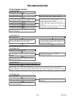
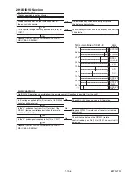
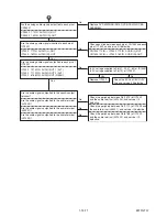
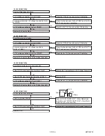
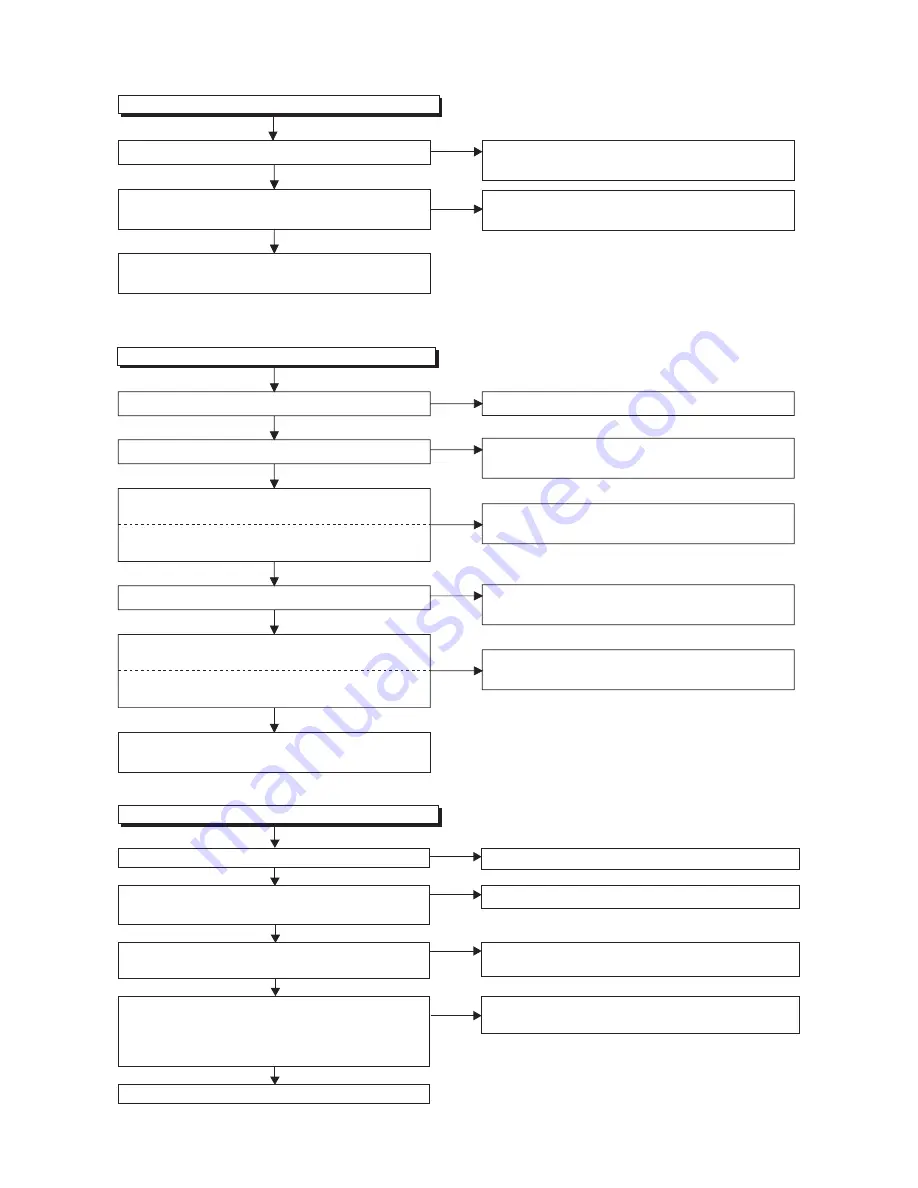
The fluorescent display tube does not light up.
Is 5V voltage supplied to Pin(13,43) of IC612?
Is approximately -24V to -28V voltage supplied to
Pin(30) of IC612?
Is there approximately 500kHz oscillation to
Pin(5) of IC612?
Are the filament voltage applied between Pin(1)
and Pin(24) of the fluorescent display tube?
Also are negative voltage applied between these pins
and GND?
Replace the fluorescent display tube.
Check the ECO+5V line and service it if defective.
Check the -FL line and service it if defective.
Check R618, IC612 and their periphery, and service it
if defective.
Check the power circuit, D1103, D1108, R1106, R1192,
C1110 and their periphery, and service it if defective.
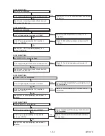
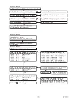
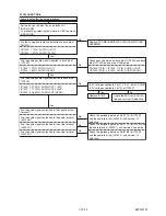
FLOW CHART NO.21
Check IC1103 and their periphery, and service it if
defective.
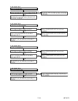
FLOW CHART NO.19
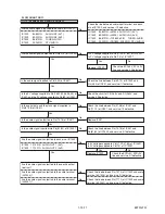
P-ON+1.8V is not outputted.
Is 2.5V voltage supplied to pin(1) of IC1103?
No
Yes
Yes
Check D1033 and their periphery, and service it if
defective.
No
Check IC3607(IC3608) and their periphery, and
service it if defective.
No
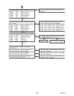
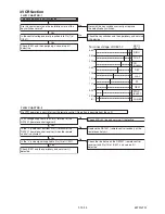
Is 5V voltage supplied to Pin(4) of CN6001?
When IC3607 is used:
Is 5V voltage outputted to Pin(8) of IC3607?
When IC3608 is used:
Is 5V voltage outputted to Pin(5) of IC3608?
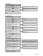
FLOW CHART NO.20
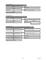
USB+5V is not outputted.
Is resistance value of both end to F6001 infinity?
Replace F6001.
Yes
No
Yes
Check CN3604 and their periphery, and service it if
defective.
Yes
Check Q1119 and their periphery, and service it if
defective.
Is 0V voltage outputted to Pin(1) of CN3605?
No
Yes
No
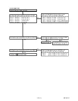
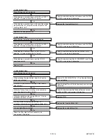
When IC3607 is used:
Is 3.3V voltage supplied to Pin(4) of IC3607?
When IC3608 is used:
Is 3.3V voltage supplied to Pin(3) of IC3608?
Yes
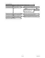
Replace DVD MECHANISM & DVD/HDD MAIN
CBA ASSEMBLY.
Is the "H" pulse (approximately 5V) inputted to
the base of Q1109?
Check the REG-CONT signal line, and service it if
defective.
No
Check CN6002 and their periphery, and service it if
defective.
Содержание TD6D-M101
Страница 16: ...1 7 4 E3TFGDC S 24 S 23 S 25 18 VCR Chassis Unit 17 Power SW CBA Desolder Lead with blue stripe Fig D7...
Страница 61: ...1 15 3 E3TFGSCAV1 AV 1 10 Schematic Diagram VCR Section...
Страница 63: ...1 15 5 E3TFGSCAV3 AV 3 10 Schematic Diagram VCR Section...
Страница 64: ...1 15 6 E3TFGSCAV4 AV 4 10 Schematic Diagram VCR Section...
Страница 65: ...1 15 7 E3TFGSCAV5 AV 5 10 Schematic Diagram VCR Section...
Страница 66: ...1 15 8 E3TFGSCAV6 AV 6 10 Schematic Diagram VCR Section...
Страница 67: ...1 15 9 E3TFGSCAV7 AV 7 10 Schematic Diagram VCR Section...
Страница 68: ...1 15 10 E3TFGSCAV8 AV 8 10 Schematic Diagram VCR Section...
Страница 69: ...1 15 11 E3TFGSCAV9 AV 9 10 Schematic Diagram VCR Section...
Страница 70: ...1 15 12 E3TFGSCAV10 AV 10 10 Schematic Diagram VCR Section...
Страница 73: ...1 15 15 Rear Jack Schematic Diagram VCR Section E3TFGSCRJ...
Страница 79: ...1 15 21 E3TFGSCD6 DVD HDD Main 6 7 Schematic Diagram DVD HDD Section...
Страница 81: ...1 15 23 E3TFGSCDTV DTV Module Schematic Diagram DVD HDD Section...
Страница 82: ...1 15 24 E3TFGSCSATA SATA Schematic Diagram...
Страница 107: ...TD6D M101 E3TFGEH 2013 04 22...

