9100A-017
7-2
******************************************************************************
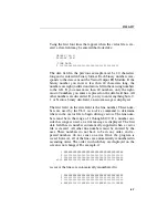
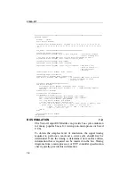
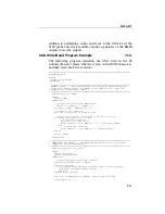
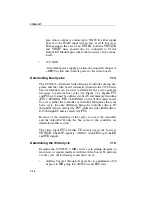
program example
devname - "/mod1"
reset device devname
setword device devname, word 1, as_pins "1 2 3 4 5 6 7 8 9 10 11 12 13 14
15 16 17 18 19 20 21 22 23 24 25 26 27 28 29 30 31 32 33 34 35 36 37 38 39
40"
low_word = "0000000000000000000000000000000000000000"
! *****Setup Output Section*****
writeword device devname, word 1, patt low_word ! initialize outputs
! before loadinq file
! vec_hilo is 40 pins wide 8192 vectors deep alternating hi and lo
vectorload device devname, file "/hdr/vector/vec_hilo"
clockfreq device devname, freq "1MHz"
syncoutput device devname, mode "intfreq"
edgeoutput device devname, start "at_vectordrive" ! stop don't care
! clock is always "+"
! for syncoutput=
! "intfreq"
enableoutput device devname, mode "always"
! *****Setup Input Section*****
counter device devname, mode "transition"
sync device devname, mode "capture" ! in "capture" mode start is forced
! at arm, clock edge is fixed,
! stop don't care
! *****Drive and Measure Responses*****
arm device devname
vectordrive device devname, startmode "now", vector 1
loop until (drivepoll device devname) = 3 ! ensure driving complete
end loop
readout device devname
! *****Process the Results*****
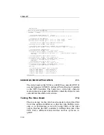
for pinnum = 1 to 40
alvl = level device devname, pin pinnum, type "async"
slvl = level device devname, pin pinnum, type "clocked"
cnt = count device devname, pin pinnum
crc = sig device devname, pin pinnum
! if not expected results, display them
if ((alvl <> 5) or <slvl <> 5> or (cnt <> 4096) or (crc <> $BC67)) then
print "Pin" + str (pinnum,10) + "ALVL = "+ str (alvl,10) +
" SLVL - " + str (slv1,10) +" CNT " + str lent,10) +
" CRC = " + str (crc, 16)
end if
next
clearoutputs device devname
end program
******************************************************************************
BUS EMULATION
7.2.
The Vector Output I/O Module can provide bus-cycle emulation
for many popular buses for testing non-microprocessor based
UUTs.
To obtain the simplest level of emulation, the signal timing
required to perform a read and a write cycle should first be
determined. Once the timing is determined, data and/or address
information that is required can be inserted on the bus. Timing
diagrams from a microprocessor or UUT controller specification
sheet typically provide this information.
Содержание 9100A Series
Страница 6: ...vi ...
Страница 8: ...viii ...
Страница 10: ...x ...
Страница 14: ...9100A 017 1 4 ...
Страница 24: ...9100A 017 3 6 ...
Страница 44: ...9100A 017 5 4 ...
Страница 58: ...9100A 017 6 14 ...
Страница 83: ...A 1 Appendix A New TL 1 Commands ...
Страница 84: ...9100A 017 A 2 ...
Страница 87: ...clockfreq 3 For More Information The Overview Of TL 1 section of the Programmer s Manual ...
Страница 88: ...clockfreq 4 ...
Страница 91: ...drivepoll 3 For More Information The Overview Of TL 1 section of the Programmer s Manual ...
Страница 92: ...drivepoll 4 ...
Страница 104: ...vectordrive 4 ...
Страница 107: ...vectorload 3 For More Information The Overview Of TL 1 section of the Programmer s Manual ...
Страница 108: ...vectorload 4 ...
Страница 116: ...9100A 017 C 2 ...
Страница 117: ...9100A 017 C 3 ...
Страница 118: ...9100A 017 C 4 ...


