background image


INP-TN512878-E

 17


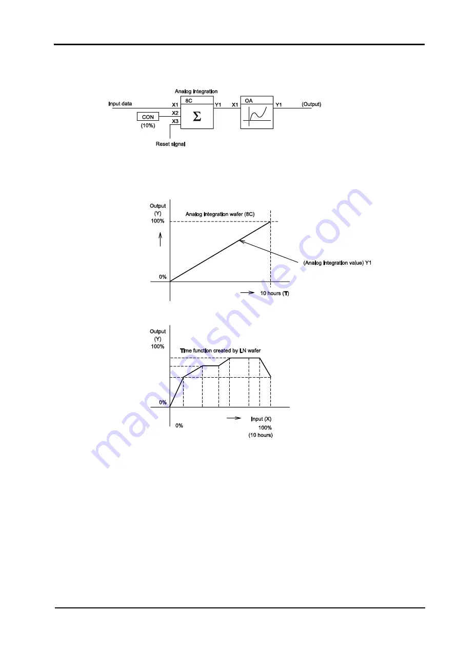
4.6  Method to create time function circuit using analog integration 

wafer and N wafer 


Figure 4-12 


It is possible to create a time function generator by combining an analog integration wafer and a 
linearize wafer.   
In the example shown above, when a value of 10% is set in constant input (X

2

) of an analog 

integration wafer (8C), the analog integration wafer integrates analog value of 100% in 10 hours, and 
the input of the linearize wafer changes by 0 to 100% in 10 hours.    It is possible to create a time 
function of 10 hours by setting a function in the linearize wafer. 

Содержание CC-M

Страница 1: ...INP TN512878 E COMPACT CONTROLLER M CC M TYPE PDA3 Application Manual Instruction Manual ...

Страница 2: ...is requested to keep the instruction manual After reading the manual it must be kept at a place always accessible by personnel in charge of its operation An arrangement must be taken so that the instruction manual will be handed over to the end user The contents of this manual have been prepared carefully However it should be noted that Fuji is not responsible for any loss caused indirectly from e...

Страница 3: ...y a power voltage matching the rating For avoiding electric shock maloperation and device troubles do not turn on power until all installation and wiring have ended The instrument is not an intrinsically safe explosion proof type Do not use it in atmosphere of combustible or explosive gases Never disassemble retouch remodel nor repair the instrument Otherwise abnormal operation electric shock or f...

Страница 4: ...ment of the temperature sensor out from the system 3 The short circuit in the thermocouple wiring 4 Valve or switch contact point outside the system is locked to keep heating on In any application in which it is apprehended that physical injury or destruction of equipment might occur we recommend to install an independent safeguard equipment to prevent over temperature which shut down the heating ...

Страница 5: ...is exerted to the main unit Splashed with water oil chemical steam or vapor Exposed to dust salt or iron excessively Inductive disturbance is so excessive as to easily produce electrostatic charge magnetic field or noise A heat accumulation occurs by radiation heat etc Install this controller on the panel so as not to apply stress to the case otherwise it may result in damage to the case If dipped...

Страница 6: ...ntrol 5 2 2 2 Bumpless changeover circuit with inverse arithmetic operation function 6 2 2 3 Bumpless changeover circuit using primary integration circuit 7 2 2 4 Bumpless changeover circuit using pulse width integration wafer 06 8 3 HOW TO HOLD OUTPUT VALUE MV 9 3 1 Method to input external signal forced manual SMAN 9 3 2 Method to input external signal EX MV 9 3 3 Method to stop addition of MV v...

Страница 7: ... 5 METHOD FOR MATERIALIZATION OF VARIOUS ADVANCE CONTROLS 21 5 1 Selective control auto selector 21 5 1 1 Method to make selection by outputs of primary integration wafer and secondary integration wafer 22 5 1 2 Method to make selection by velocity control type outputs of primary PID wafer and secondary PID wafer 23 5 2 Variable gain control 24 5 2 1 Variable gain by LIN wafer 25 5 2 2 Variable ga...

Страница 8: ...ntroller M hereinafter abbreviated as CC M for materializing a sophisticated measurement control system using CC M It also describes general precautions and typical applications that constitute a system Make best use of this Application Manual for materializing more sophisticated functions using CC M FOREWORD ...

Страница 9: ......

Страница 10: ... of a wafer that is mounted before oneself On the contrary by making use of this fact it is possible to use data that is earlier by one sampling period 0 2 second for example 1 2 Correspondence of external signals and internal signals 1 Voltage of 1 to 5V or current of 4 to 20mA corresponds to wafer of 0 00 to 100 0 Arithmetic operation by the internal control block is executed in the range of 327...

Страница 11: ...thmetic operations 300 100 300 50 50 100 50 100 50 Addition 50 30 20 200 50 150 Subtraction Multiplication 100 100 100 01 0 1 1 06 74 66 66 11 111 60 30 200 100 100 20 300 60 Division Square root 50 20 10 100 200 200 42 141 200 20 173 300 10 1 0 5 ...

Страница 12: ... 4 Modes and output signals of controller Figure 1 1 What requires balance operation for bumpless changeover out of these changeovers is Changeover from a mode other than EX M mode to EX M mode See section 1 5 Important ...

Страница 13: ...t the time of changeover of operation output to EX M 1 Method to gradually bring close by ramp output wafer Figure 1 2 When an EX M external output setup command enters the output MV varies by inclination CONT determined by the ramp wafer Bump impact is prevented as a result ...

Страница 14: ... Case where R SV is an internal signal caser where primary PID control and secondary PID control are used 2 2 1 Bumpless changeover circuit of ordinary cascade control Wafer wire connection is performed as shown below in case of ordinary cascade control In this case when auto A mode is selected 2ND LS signal is 0 01 ON and the input of primary integration wafer 23 has been changed to the value of ...

Страница 15: ...nction In case where an arithmetic operation circuit is located between primary PID and secondary PID if its arithmetic operation is simple Figure 2 2 bumpless changeover can be accomplished by feedback to the primary integration circuit by way of the inverse arithmetic operation circuit ...

Страница 16: ...tant value control is good in the A mode and steady state is produced secondary PV and secondary SV are almost matched When the deviation between this PV and 41 wafer output Y4 R SV PV is made small the R SV value and the secondary SV value are almost matched For this purpose the R SV value is controlled by using the output of R SV PV in integration I term of primary PID arithmetic operation in th...

Страница 17: ...determined by the integration time of primary PID and there are cases where bumpless changeover cannot be accomplished within a short length of time In such a case bumpless changeover can be accomplished within a short length of time if the difference between R SV and 2ND SV is integrated by pulse width integration wafer 06 and if feedback of the result is made to primary integration wafer 23 The ...

Страница 18: ...id In this case call the ALARM CONNECT screen out of the OUT CONNECT screen and register DI terminal mode in SMAN REQ 3 2 Method to input external signal EX MV Input a DI signal of EX MV specified opening mode from outside Figure 3 1 When an output signal is input through the input terminal of EX MV the then output value is held 3 3 Method to stop addition of MV value Figure 3 2 When integration v...

Страница 19: ...urning the output Y1 of the changeover wafer 67 to the input X1 Figure 4 1 4 1 2 Sample hold circuit using pulse generation wafer Figure 4 2 The value is held at the time when the pulse generator wafer 88 is ON Note Sample hold wafer DO is also available 4 Method for materialization of various functions using wafers of various types ...

Страница 20: ... 1 to 0 When two flip flop wafers 67 are used they can be used as R S flip flop 4 1 4 Changeover of digital signal A changeover wafer can also handle changeover of digital signal When it is wanted to set the digital signal by a constant use 0 00 instead of 0 OFF and use 0 01 instead of 1 ON A changeover wafer is capable of changing both analog and digital signals Note Flip flop wafer A5 is also av...

Страница 21: ... 2 SEC only 4 2 2 Method to seize fall of input Figure 4 5 Seize the fall of the input and turn OFF a basic period 0 2 SEC only These methods are to read input X1 X2 X3 by the first basic period 0 2 SEC and to direct them to Y1 to Y4 In case feedback of Y1 to X3 is made as illustrated above X3 changes from 1 to 0 with a lag of 0 2SEC One shot is created by making use of this lag Figure 4 6 ...

Страница 22: ...ng timer and logical wafer Figure 4 7 It is possible to create one shot multiple circuits by the combination of timer and E OR EXCLUSIVE OR The ON time can be set arbitrarily by the timer set time T Logic of E OR 1 1 0 0 0 0 1 0 1 0 1 1 ...

Страница 23: ... if the input enters by the inclination of time T1 curve a c In this case output Y2 of the ramp wafer produces a match signal at point a 0 and point c 100 and produces a mismatch signal at other points When the input of the ramp wafer arrives by time T2 under the same conditions the output of the ramp wafer is produced by the inclination of time T2 curve a d In this case output Y2 of the ramp wafe...

Страница 24: ...ime wafers it is done as shown below Figure 4 10 Note With a dead time wafer even if setting of dead time L exceeds the setting range i e 2 minutes it is limited to 2 minutes internally Furthermore even if the dead time is set a minus value it is limited to 0 minute The above example shows a case to produce a dead time of 3 minutes using dead time wafers 1 and 2 When dead time L of dead time wafer...

Страница 25: ...ht time 40 seconds is ON by the comparison wafer 08 in this example While said pulse is ON the flow rate for one pulse 1T 90t H 40 seconds is subtracted from the analog integration wafer 8C by way of the subtraction wafer 63 The values of constant CON6 90t H 180 and CON9 40 seconds are determined arbitrarily so that their product becomes one pulse weight that is 1t If the output pulse width 40 sec...

Страница 26: ...og integration wafer and a linearize wafer In the example shown above when a value of 10 is set in constant input X2 of an analog integration wafer 8C the analog integration wafer integrates analog value of 100 in 10 hours and the input of the linearize wafer changes by 0 to 100 in 10 hours It is possible to create a time function of 10 hours by setting a function in the linearize wafer ...

Страница 27: ...create segmented lines 17 to 32 by LIN2 and to then create 32 segmented lines by two LIN wafers The example shown above indicates a case where changeover to segmented lines on LIN2 side when the input becomes 50 At the 50 point which is the changeover point it is necessary to set the same value input value at the end point of LIN1 and start point of LIN2 ...

Страница 28: ... setting wafer is automatically held in the reset state state where reset terminal X2 of the program wafer is 1 When the external momentary signal DI2 changes as 0 1 0 the reset input X2 of the program wafer changes from 1 to 0 and the program wafer starts up The reset input X2 of the program wafer is held at 0 at this time When the program terminates the end signal Y4 of the program wafer changes...

Страница 29: ...e wafer located before the secondary integration wafer 43 so that it is an inverse function of LIN for bulb compensation Set the characteristics of the LIN so as to represent the valve opening change rate against the flow rate instead of valve characteristics themselves Figure 4 16 ...

Страница 30: ...e of control of the outflow rate for a tank to keep the flow rate at a fixed level is the prime objective But the liquid level should be kept in a certain range or less on the other hand In such a case selective control auto selector of flow rate and liquid level is executed Flow rate control to keep the outflow rate at a fixed level is selected in the normal state But when the liquid level is dev...

Страница 31: ... is commonly used changeover between primary PID and secondary PID is made by changeover signal and either one controller is selected Since feedback of the output signal is made to both of primary integration wafer 23 and secondary integration wafer 43 in this case Balanceless and bumpless changeover can be achieved at any time by a changeover signal ...

Страница 32: ...in this case is such that the integration wafer 43 and output wafer 44 of secondary PID are commonly used and changeover is made by outputs of primary PID wafer 22 and secondary PID wafer 42 Since both of PID wafers 22 42 are of velocity control type arithmetic operation MV balanceless and bumpless changeover can be achieved at any time by a changeover signal ...

Страница 33: ...cessary to pay attention as the effect is different between the case where proportional band P is changed and the case where the proportional term is changed The method to change the output of the PID wafer is better for so called variable gain To change the integration gain multiply the gain to the integral term X2 of the integration wafer Integration I cut action occurs when the input is changed...

Страница 34: ...ging the PV value The gain is changed by LIN wafer and multiplication wafer To change the gain by deviation DV make connection as shown by broken lines In this case set the gain curve produced by actual process value PV value or deviation DV value to the LIN wafer Case where process gain changes by PV value Figure 5 6 ...

Страница 35: ...onstant set in both of primary PID wafer and secondary PID wafer 42 in case primary PID Control sequence is not used 5 2 3 Deviation square type PID control Figure 5 8 Deviation square type PID is to execute control in proportion to the square of the deviation It is used for PH control or the like in general and is largely different from ordinary PID control Figure 5 9 ...

Страница 36: ...ed that even if fuel variation can be controlled in the cascade loop the temperature would naturally vary to a major extent If the supply flow rate can be measured at the inlet it is possible to detect variation of demand in advance and it is possible to compensate and control the supply fuel in advance before temperature change occurs in the furnace Temperature deviation will not arise if the val...

Страница 37: ...ation wafer 43 at this time Static feed forward is effective in general when the disturbance element is relatively small Figure 5 11 5 3 2 Dynamic feed forward Lead and lag elements of are executed to the disturbance signal and are added to the control output MV Note that the unit of setting is different between lead element T2 and lag element T1 T1 minute T2 second As the change component of the ...

Страница 38: ...t PID control Smith s compensation etc are available as methods for dead time control using CC M 5 4 1 Sampling control Sampling control is provided as a standard function of CC M and it can be materialized only by setting the sampling time With PID control setup can be made by the time of DT parameter 0 1SEC to 9999 9SEC 0 1SEC interval default value 0 2SEC in the PID parameter setting screen for...

Страница 39: ...od It is more effective than sampling control for a process of relatively large noise With CC M this control can be materialized by the combination of a changeover wafer and a pulse generation wafer PID is executed during the ON time of the pulse generation wafer and intermittent PID control is executed in the hold status during the OFF time As the wafer connection an intermittent circuit is inser...

Страница 40: ...adding internal compensation circuit G1 1 e LS to a system having dead time of GP e LS in the process deformation to such a form that the system viewed from the controller controls the system equivalently without dead time Thus the process can be controlled as what is without dead time Figure 5 15 ...

Страница 41: ...r connection in Smith s dead time compensation control circuit Figure 5 16 The wafer connection chart indicated above shows a case where the process transfer function is known as being G S and dead time L can be easily measured 1 1 TS ...

Страница 42: ......

Страница 43: ...r 11 2 Osaki 1 chome Shinagawa ku Tokyo 141 0032 Japan http www fesys co jp eng Instrumentation Div International Sales Dept No 1 Fuji machi Hino city Tokyo 191 8502 Japan Phone 81 42 585 6201 6202 Fax 81 42 585 6187 http www fic net jp eng ...

Отзывы: