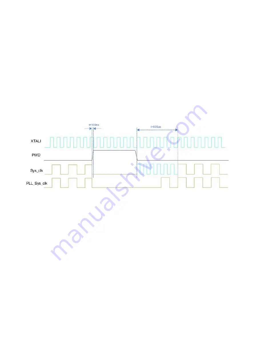
When the GPIO is pulled low again, the chip is in normal operation mode. In this case, the ByPass
internal PLL needs to be used to provide the clock through the crystal XTALI direct HR_C6000.
After waiting for more than 500μs. s, switch to the internal PLL to provide the HR_C6000 working
clock.
As shown in the figure, XTALI is the crystal input clock signal, PWD is the sleep signal of
HR_C6000, Sys_clk is the working clock of HR_C6000; PLL_Sys_clk is the clock obtained by
dividing the frequency of HR_C6000 after the PLL output.
The MCU configuration PWD is high, and the PWD is stable after 100ns. At this time, the
HR_C6000 internal clock is all cleared. After the PWD is pulled low again, the working clock needs
to be switched to XTALI. After waiting for the PLL to stabilize the output of the divided
PLL_Sys_clk, switch to the PLL. The divided output clock has a settling time greater than 500μs. s.
Figure 4.9 Schematic diagram of PWD control timing and working clock switching requirements
HR_C6000 provides 4 interrupt pins, the interrupt low pulse is valid, the pulse width is 3 system
working clocks (Sys_clk, 9.8304MHz), SYS_INTER is to receive the indication interrupt of the
system receiving and transmitting information, and the sending process and receiving process
prompt the MCU status or control. TIME_SLOT_INTER is a 30ms time slot interrupt. This
interrupt is generated cyclically after the HR_C6000 establishes a synchronization time slot. It is
used to establish a TDMA time slot structure for the MCU. RF_TX_INTER and RF_RX_INTER
are RF transceiver switching control interrupts. It is generated during the switching process to
facilitate accurate and timely control of the RF channel by the MCU. RF_TX_INTER and
RF_RX_INTER are alternately generated according to the period of 30ms. In order to facilitate the
early start of the RF transmission control, register Reg0x12 can be set to control RF_TX_INTER
and register Reg0xC0 to control RF_RX_INTER. The advance of 0ms can be configured with
respect to the 30ms boundary.
OMISSIS
Figure 4.10 Schematic diagram of RF_TX_INTER and RF_RX_INTER generation
Table 4.2 RF_TX_INTER Interrupt Control Register Address Description
Содержание HR C6000
Страница 5: ...1 Chip block diagram OMISSIS ...
Страница 6: ...2 Chip pin 2 1 Pin map OMISSIS HR_C6000 pin diagram picture is missing ...
Страница 51: ......


