background image


EDM01-14 DAG 3.6D Card User Guide 


©2005


22 

Version 10: May 2006


5.0 SYNCHRONIZING CLOCK TIME 

Description 

The Endace DAG range of products come with sophisticated time 

synchronization capabilities, in order to provide high quality timestamps, 

optionally synchronized to an external time standard. 


The system that provides the DAG synchronization capability is known as 

the DAG Universal Clock Kit (DUCK).  


An independent clock in each DAG card runs from the PC clock.  A 

card’s clock is initialised using the PC clock, and then free-runs using a 

crystal oscillator.   


Each card's clock can vary relative to a PC clock, or other DAG cards. 


DUCK 

configuration 

The DUCK is configured to avoid time variance between sets of DAG 

cards or between DAG cards and coordinated universal time [UTC].   


Accurate time reference can be obtained from an external clock by 

connecting to the DAG card using the synchronization connector, or the 

host PCs clock can be used in software as a reference source without 

additional hardware. 


Each DAG card can also output a clock signal for use by other cards. 


Common 

synchronization 

The DAG card synchronization connector supports a Pulse-Per-Second 

(PPS) input signal, using RS-422 signalling levels.  


Common synchronization sources include GPS or CDMA (Cellular 

telephone) time receivers.   


Endace produces the TDS 2 Time Distribution Server modules and the 

TDS 6 units that enable multiple DAG cards to be connected to a single 

GPS or CDMA unit.  


More information is on the Endace website, 

http://www.endace.com/accessories.htm

, or the TDS 2/TDS 6 Units 

Installation Manual. 


In this chapter 

This chapter covers the following sections of information. 


Configuration Tool Usage 


Time Synchronization Configurations 


Synchronization Connector Pin-outs 


Содержание DAG 3.6D

Страница 1: ......

Страница 2: ...7 839 0543 support endace com www endace com Endace USA Ltd Suite 220 11495 Sunset Hill Road Reston Virginia 20190 United States of America Phone 1 703 382 0155 Fax 1 703 382 0155 support endace com...

Страница 3: ...ral Communications Commission FCC Rules These limits are designed to provide reasonable protection against harmful interference when the equipment is operated in a commercial environment This equipmen...

Страница 4: ...ty 7 3 2 Interpreting DAG 3 6D Card LED Status 8 3 3 DAG 3 6D Card LED Display Functions 9 3 4 Configuration in WYSYCC style 10 3 5 DAG 3 6D Card Capture Session 10 3 6 Inspect Interface Statistics 12...

Страница 5: ...EDM01 14 DAG 3 6D Card User Guide 2005 ii Version 10 May 2006...

Страница 6: ...tion The purpose of this DAG Card installation guide is to describe Installation of Operating System and Endace Software Confidence Testing DAG 3 6D Card Running Data Capture Software Synchronizing Cl...

Страница 7: ...fferent interfaces this manual describes the DAG 3 6D Dual DS3 T3 co axial interface Figure Figure 1 1 shows the DAG 3 6D card Figure 1 1 DAG 3 6D Card 1 3 DAG 3 6D Card Architecture Description Becau...

Страница 8: ...he DAG 3 6D card major components and process flow Figure 1 2 DAG 3 6D Card Major Components and Process Flow Time stamped packet or cell records are stored in a FIFO The DAG 3 6D can demap either ADM...

Страница 9: ...support endace com 1 5 DAG 3 6D Card System Requirements Description The DAG 3 6D card and associated data capture system minimum operating requirements are PC at least Pentium II 400 MHz Intel 440BX...

Страница 10: ...his section This section covers the following topics of information Installation of Operating System and Endace Software Insert DAG 3 6D Card into PC DAG 3 6D Card Port Connectors 2 1 Installation of...

Страница 11: ...d with screw Step 4 Power Up Computer 2 3 DAG 3 6D Card Port Connectors Description There are two metal co axial BNC connectors on the DAG 3 6D card The top co axial is Port A furthest from the PCI sl...

Страница 12: ...wer is slightly out of range then an increased bit error rate will be experienced If the power is well out of range then the system will be unable to lock to the PDH frames Signal source specification...

Страница 13: ...tenuator if the level is too high or an amplifier if the level is too low Splitters Passive splitters usually have their insertion losses marked on the package or in the accompanying documentation A 5...

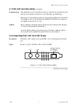
Страница 14: ...G 3 6D Card LED Display Functions Description On the DAG 3 6D series of cards LEDs 1 and 2 display when powered up When DS3 signals are applied LEDs 6 and 8 should go out LEDs 5 and 7 should come on T...

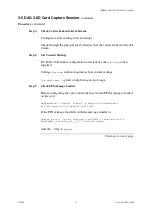
Страница 15: ...not add 20dB extra gain to Rx 3 5 DAG 3 6D Card Capture Session Description The DAG 3 6D card uses the SONET PDH ATM physical layer interface device to support capturing of ATM The card supports the...

Страница 16: ...ation and statistics the dagthree tool is supplied Calling dagthree without arguments lists current settings The dagthree h prints a help listing on tool usage Step 5 Check FPGA Image Loaded Before co...

Страница 17: ...s configured for c bit nom23 framing mode but m23 framing is required removing or adding the no prefix will change the setting Type dag endace dagthree d dag0 m23 linkA noreset noadm m23 nohighgain no...

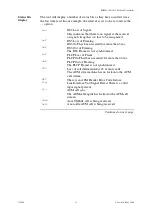
Страница 18: ...for more than 3 ms OoF DS3 Out of Framing The DS3 Framer is not synchronized LoF PLCP Loss of Frame PLCP OoF had been asserted for more than 3 ms OoE PLCP Out of Framing The PLCP Framer is not synchr...

Страница 19: ...there is no valid signal input is A LoS LoF OoF LoF OoF LCD HEC Fix Sig Syn Idle Cell 1 1 1 1 1 1 0 0 0 0 0 0 1 1 1 1 1 1 0 0 0 0 0 0 1 1 1 1 1 1 0 0 0 0 0 0 Status bits The PLCP LoF and OoF status b...

Страница 20: ...ration 3 Host PC operating system version 4 DAG software version package in use 5 Any compiler errors or warnings when building DAG driver or tools 6 For Linux and FreeBSD messages generated when DAG...

Страница 21: ...EDM01 14 DAG 3 6D Card User Guide 2005 16 Version 10 May 2006...

Страница 22: ...EDM01 14 DAG 3 6D Card User Guide 2005 17 Version 10 May 2006...

Страница 23: ...talled drv dagload tools dagld d dag0 x xilinx dag36pci erf bit xilinx dag36atm erf bit The integrity of the card s physical layer is then set and the integrity of the physical layer to both DAG cards...

Страница 24: ...and packet records are lost When the PC buffer fills the message kernel dagN pbm safety net reached 0xNNNNNNNN is displayed on the PC screen and printed to log var log messages The Data capture LED a...

Страница 25: ...2Mbps rates and above 128MB or more may be required per card To change the amount of memory reserved edit the file etc modules If the Endace Install CD has been used it will include this section For D...

Страница 26: ...EDM01 14 DAG 3 6D Card User Guide 2005 21 Version 10 May 2006...

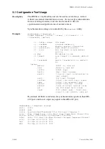
Страница 27: ...C Accurate time reference can be obtained from an external clock by connecting to the DAG card using the synchronization connector or the host PCs clock can be used in software as a reference source w...

Страница 28: ...hold health threshold in ns default 596 Option default RS422 in none out none None in none out rs422in RS422 input hostin Host input unused overin Internal input synchronize to host clock auxin Aux in...

Страница 29: ...ock If a PC is running NTP to synchronize its own clock then the DUCK clock is less smooth because the PC clock is adjusted in small jumps However overall the DUCK clock does not drift away from UTC T...

Страница 30: ...rrect then one card is configured as the clock master for the other Locking cards together Although the master card s clock will drift against UTC the cards are locked together The cards are locked to...

Страница 31: ...77ppb Worst Phase 88424ns crystal Actual 49999354Hz Synthesized 16777216Hz input Total 87464 Bad 0 Singles Missed 0 Longest Sequence Missed 0 start Wed Apr 27 14 27 41 2005 host Thu Apr 28 14 59 14 20...

Страница 32: ...ad 0 Singles Missed 1 Longest Sequence Missed 1 start Thu Apr 28 14 55 20 2005 host Thu Apr 28 14 59 06 2005 dag Thu Apr 28 14 59 06 2005 Connecting time distribution server The TDS 2 module connects...

Страница 33: ...socket connector pin outs Figure 6 1 RJ45 Plug and Socket Connector Pin outs Out pin connections Normally the GPS input should be connected to the A channel input pins 3 and 6 The DAG card can also ou...

Страница 34: ...EDM01 14 DAG 3 6D Card User Guide 2005 29 Version 10 May 2006...

Страница 35: ...able 7 1 shows the generic variable length record The diagram is not to scale timestamp timestamp type flags rlen lctr wlen rlen 16 bytes of record Table 7 1 Generic Variable Length Record Data format...

Страница 36: ...s record Records can be lost between the DAG card and memory hole due to overloading on PCI bus The counter starts at zero and sticks at 0xffff Wlen wire length Packet length including some protocol o...

Страница 37: ...January 1970 The high 32 bits contain the integer number of seconds while the lower 32 bits contain the binary fraction of the second This allows an ultimate resolution of 2 32 seconds or approximatel...

Страница 38: ...example code showing how a 64 bit ERF timestamp erfts can be converted into a struct timeval representation tv unsigned long long lts struct timeval tv lts erfts tv tv_sec lts 32 lts lts 0xffffffffULL...

Отзывы: