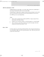
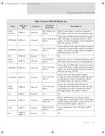
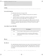
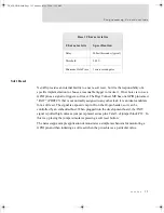
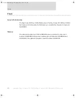
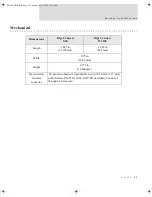


4 3
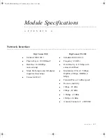
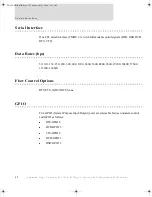
M o d u l e S p e c i f i c a t i o n s
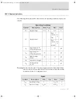
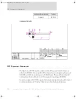
DC Characteristics
The following tables provide DC characteristics for operating conditions, inputs, and
outputs.
Warning
The rise time of your 3.3V power supply needs to be faster than 140ms.
That is it needs to be less than 140ms. If the rise time is more than 140ms,
it could lead to the 3-1-3 diagnostic error.
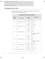
Operating Conditions
Symbol
Description
Min
Typ
Max
Unit
V
CC
Supply Voltage
3.14
3.3
3.45
V
I
CC
Supply Current
—
—
Digi
Connec
t
EM
27
0
mA
Digi
Connec
t
Wi-EM
40
0
I
IL
Input Current as “0”
(57K pull-up resistor)
—
—
57
µ
A
I
IH
Input Current “1”
(57K pull-up resistor)
-10
—
10
µ
A
I
OZ
HighZ Leakage
Current
-10
—
10
µ
A
I
OD
Output Drive Strength
—
—
2
mA
C
IO
Pin Capacitance
(V
O
=0)
—
—
4
pF
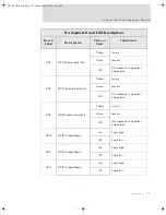
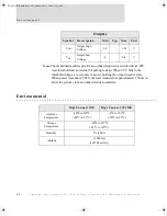
Inputs
Symbol
Description
Min
Typ
Max
Unit
V
IH
Input High Voltage
2
—
V
CC
+0.3
V
V
IL
Input Low Voltage
V
SS
-0.3
—
0.2*V
CC
V
DC_ME-HWR.book Page 43 Thursday, July 1, 2004 11:12 AM
Содержание Digi Conntect ME
Страница 1: ...TM TM 90000631_A DC_ME HWR book Page 1 Thursday July 1 2004 11 12 AM...
Страница 2: ...DC_ME HWR book Page 2 Thursday July 1 2004 11 12 AM...
Страница 4: ...DC_ME HWR book Page 4 Thursday July 1 2004 11 12 AM...
Страница 47: ...47 M o d u l e S p e c i f i c a t i o n s Bottom DC_ME HWR book Page 47 Thursday July 1 2004 11 12 AM...
Страница 63: ...DC_ME HWR book Page 63 Thursday July 1 2004 11 12 AM...
Страница 64: ...DC_ME HWR book Page 64 Thursday July 1 2004 11 12 AM...


