background image

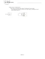
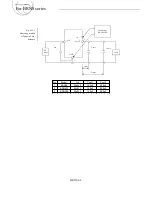
(4) Reverse input voltage protection

Avoid the reverse polarity input voltage. It will damage the power supply.
It is possible to protect the unit from the reverse input voltage by installing an external
diode as shown in Fig.3.2.2.

Fig. 3.2.2

Reverse input voltage

protection

BRNS 3-3

Applications manual

For BRNS series

Содержание CHS200483R3

Страница 1: ...VER1 5 Qualification of BRNS BRFS BRDS series Point of Load applications to Intermediate Bus Architecture Page BRNS Page BRFS BRDS Page BRFS BRDS Page CHS and BR...

Страница 2: ...e voltage BRNS 4 7 Rise time BRNS 4 8 Derating BRNS 4 9 5 Adjustable voltage range BRNS 5 1 6 Protect circuitry BRNS 6 1 Overcurrent protection BRNS 6 1 7 Remote ON OFF BRNS 7 1 8 Remote sensing BRNS...

Страница 3: ...Fig 1 1 Pin connection for BRNS bottom view Table 1 1 Pin connection and function of BRNS a BRNS6 12 b BRNS20 BRNS 1 1 2 1 Pin configuration 1 Pin configuration Applications manual For BRNS series...

Страница 4: ...ple distance between the line pattern layout and the unit Also avoid placing the DC output line pattern underneath the unit because it may increase the output noise Lay out the pattern away from the u...

Страница 5: ...n for reflow of BRNS series Please make sure that the temperature of board s pattern near by VOUT and GND terminal While soldering having vibration or impact on the unit should be avoided because of s...

Страница 6: ...size for stencil openings is shown in Fig 2 4 1 Fig 2 4 1 Recommended size for stencil openings Top view Dimensions in mm inches Recommended stencil thickness is 0 12mm BRNS 2 3 a BRNS6 12 b BRNS20 Ap...

Страница 7: ...ept under uncontrolled condition which is 30 60 RH or higher Original reels are not heat resistant Please move them to heatresistant trays in preparation to bake To check moisture condition in the pac...

Страница 8: ...s to turn on the power supply GND RC VOUT S GND S S only BRNS20 Connect resistance to set the output voltage between TRM and GND Between input and output is not isolated The BRNS series handle only th...

Страница 9: ...the input side Install an external capacitor Ci between VIN and GND input pins for low line noise and for stable operation of the power supply Table 3 2 2 Recommended external input capacitor Ceramic...

Страница 10: ...rity input voltage It will damage the power supply It is possible to protect the unit from the reverse input voltage by installing an external diode as shown in Fig 3 2 2 Fig 3 2 2 Reverse input volta...

Страница 11: ...h Co and ESL of the wiring if resonance frequency and switching frequency are close Ripple and Ripple Noise are measured as shown in the Fig 3 3 2 Cin is shown in Table 3 2 2 Co1 and Co2 is shown in T...

Страница 12: ...oad Current A 60 68 76 84 92 100 0 2 4 6 Efficiency Load Current A 60 68 76 84 92 100 0 4 8 12 Efficiency Load Current A 60 68 76 84 92 100 0 4 8 12 2 1 Pin configuration 4 Applications data Input Vol...

Страница 13: ...8 76 84 92 100 0 5 10 15 20 Efficiency Load Current A 60 68 76 84 92 100 0 5 10 15 20 Efficiency Load Current A 60 68 76 84 92 100 0 5 10 15 20 Input Volt Input Volt Input Volt 14 4V 6 5V 12V Input Vo...

Страница 14: ...nse BRNS 4 3 100 s div 100 s div 100 s div 100 s div 100 mV div 100 mV div Vin 12V Vout 1 2V Cin 22 F 2 Cout 1000 F Testing Circuitry Fig 4 2 3 2 Load 50 3A Load 0 0A Load 100 6A Load 50 3A Cycle Load...

Страница 15: ...100 s div 100 s div 100 s div 100 s div Cycle Load Current 5 m t1 t2 50 s t1 t2 Vin 12V Vout 1 2V Cin 22 F 2 Cout 1000 F Testing Circuitry Fig 4 2 3 2 100 mV div 100 mV div Load 50 6 A Load 100 12A s...

Страница 16: ...00 s div 100 s div 100 s div 100 s div Cycle Load Current 5 m t1 t2 50 s t1 t2 Vin 12V Vout 1 2V Cin 22 F 3 Cout 1000 F Testing Circuitry Fig 4 2 3 2 100 mV div 100 mV div Load 50 10 A Load 100 20A s...

Страница 17: ...oad Response BRNS 4 6 Load 25mm Cout2 VIN VOUT GND DC Input Cin S 3mm Cout1 Cin 22 F 2 22 F 2 22 F 3 3 BRNS20 100 F 900 F No 1 2 Model Cout1 Cout2 BRNS6 BRNS12 100 F 900 F 100 F 900 F Oscilloscope Bw...

Страница 18: ...mV div b BRNS12 Vin 12V Vout1 2V Load Current 20A BRNS20 Vin 12V Vout1 2V Load Current 12A Oscilloscope Bw 20MHz R C R 50 C 0 01uF 1 5m 50 Coaxial cable Load 25mm Cout2 3mm Cout1 VIN VOUT GND DC Input...

Страница 19: ...g 4 4 2 Load current 0A Cin 22 F 2 Cout 100 F 47 F BRNS12 Rise at 25 200mV div 2V div 5ms div 5ms div Rise time 3 5ms Rise time 3 8ms Vin 8V Vout 0 6V Vin 12V Vout 5 5V Fig 4 4 3 Load current 0A Cin 2...

Страница 20: ...specified point be less than or equal to the temperature shown in FIG 1 Ambient temperature must be maintained at 85 or less Fig 4 5 1 Derating curve for BRNS Fig 4 5 2 Temperature measurement locati...

Страница 21: ...4 Measuring method Fig 4 5 5 Derating curve for BRNS6 at 12Vin 1 2Vout Fig 4 5 6 Derating curve for BRNS6 at 12Vin 3 3Vout BRNS 4 10 12 7mm 76mm 25 4mm BRNS20 PWB Measurement point for ambient tempera...

Страница 22: ...NS12 at 12Vin 5 5Vout BRNS 4 11 0 6 5 4 Load current A 3 2 1 40 60 80 Ambient temperature 40 20 0 20 1m s 2m s 0 40 60 80 Ambient temperature 40 20 0 20 Load current A 12 10 8 6 4 2 1m s 2m s 0 40 60...

Страница 23: ...ing curve for BRNS20 at 12Vin 5 5Vout BRNS 4 12 0 20 16 12 8 4 Load current A 40 Ambient temperature 20 0 20 40 60 80 1m s 2m s 0 40 60 80 Ambient temperature Load current A 20 16 12 8 4 40 20 0 20 1m...

Страница 24: ...a resistor Resistor Metal film type coefficient of less than 100ppm When TRM is opened output voltage is 0 6V RTRM is calculated in the following expressions Fig 5 1 1 Calculation result Fig 5 1 2 Co...

Страница 25: ...there is a possibility that the ripple voltage is high value If the ripple voltage value is problem connecting a capacitor of Table 3 3 1 value Fig 5 1 3 Operating area of BRNS series When start of DC...

Страница 26: ...whenever possible The output voltage of the power module will recover automatically when the fault causing overcurrent is corrected When the output voltage drops after OCP works the power module ente...

Страница 27: ...cification of Remote ON OFF Fig 7 1 1 Internal circuitrys of Remote ON OFF Fig 7 1 2 RC connection example ON OFF logic Between RC and GND Output voltage Optional R Positive L level 0 2 0 3V or short...

Страница 28: ...e sensing function is use Fig 8 2 1 Connection when the remote sensing is in use Twisted pair wire or shield wire should be used for sensing wire Thick wire should be used for wiring between the power...

Страница 29: ...10 Fig 9 1 1 Internal circuitry of PGood Fig 9 1 2 BRNS6 RC 5V div Vin 12V t0 5ms Max PGOOD Vout 5 5V Vout 2V div load current 0A PGOOD 2V div Cin 22uFx2 Cout 100uF 47uF 5ms div Fig 9 1 3 BRNS12 RC 5...

Страница 30: ...ing C CSEQ nF 6 TRISE ms 15 CSEQ should be less than 1 0 F At the time of start the output voltage follows the SEQ voltage Output voltage and SEQ voltage are expressed in the following calculation BRN...

Страница 31: ...you can control a start sequence of plural BRNS Fig 10 1 1 Example of sequence control If this function is unnecessary please make SEQ pin open BRNS 10 2 a The same time b The same voltage c The time...

Страница 32: ...YNC pin is shown in Fig 11 1 2 If this function is unnecessary please make SYNC pin open or short to GND Please wire the input pin of both power supplies which is synchronizing to the same pattern and...

Страница 33: ...r the power supply which output CLK started please start the synchronizing power supplies And when stop power supplies you should stop the power supply which output CLK at first The max voltage of CLK...

Страница 34: ...ilable by wiring as shown below Fig 12 2 1 Redundancy operation Even a slight difference in output voltage can affect the balance between the values of I1 and I2 Current I3 should not exceed the rated...

Страница 35: ...Fig 13 1 3 for Package form Reel The packed number is 200 Fig 13 1 1 Taping dimensions of BRNS6 12 Fig 13 1 2 Taping dimensions of BRNS20 BRNS 13 1 2 1 Pin configuration 13 Package Information Applica...

Страница 36: ...Fig 13 1 3 Reel dimensions of BRNS BRNS 13 2 Applications manual For BRNS series...

Страница 37: ...e BRFS BRDS 4 9 Ripple voltage BRFS BRDS 4 22 Rise time BRFS BRDS 4 24 Derating BRFS BRDS 4 26 Thermal simulation model BRFS BRDS 4 35 5 Adjustable voltage range BRFS BRDS 5 1 6 Protect circuitry BRFS...

Страница 38: ...40 Fig 1 1 1 Pin connection for BRFS30 40 60S bottom view Table 1 1 1 Pin connection and function of BRFS30 40 60S BRFS BRDS 1 1 2 1 Pin configuration 1 Pin configuration Applications manual For BRFS...

Страница 39: ...50 Fig 1 2 1 Pin connection for BRFS50 50L 60 100 120 150 bottom view a BRFS50 50L 60 120 b BRFS100 150 Table 1 2 1 Pin connection and function of BRFS50 50L 60 100 120 150 BRFS BRDS 1 2 Applications...

Страница 40: ...1 3 BRDS40 Fig 13 1 Pin connection for BRDS40 60S bottom view Table 13 1 Pin connection and function of BRDS40 60S BRFS BRDS 1 3 Applications manual For BRFS BRDS series...

Страница 41: ...S60 100 Fig 1 4 1 Pin connection for BRDS60 100 120 bottom view a BRDS60 120 b BRDS100 150 Table 1 4 1 Pin connection and function of BRDS60 100 120 150 BRFS BRDS 1 4 Applications manual For BRFS BRDS...

Страница 42: ...he line pattern layout and the unit Also avoid placing the DC output line pattern underneath the unit because it may increase the output noise Lay out the pattern away from the unit Avoid placing the...

Страница 43: ...d 1 BRFS100 150 d 2 BRDS100 150 BRFS BRDS 2 2 c 1 BRFS40 60S c 2 BRDS40 60S Applications manual For BRFS BRDS series...

Страница 44: ...the PCB as an adsorption point Please see Fig 2 2 1 for details of the adsorption point Fig 2 2 1 Adsorption area b BRFS50 BRFS50L BRFS BRDS 2 3 d BRFS60 BRDS60 a BRFS30 c BRFS40 BRDS40 e BRFS100 BRD...

Страница 45: ...ct on the unit should beavoided because of solder melting Please do not do the implementation except the reflow Because some parts drops please do not do reflow of the back side Fig 2 3 1 Recommended...

Страница 46: ...der uncontrolled condition which is 30 60 RH or higher Original reels are not heat resistant Please move them to heat resistant trays in preparation to bake To check moisture condition in the pack Sil...

Страница 47: ...wer supply GND RC VOUT S GND S S other model than BRFS30 40 Connect resistance to set the output voltage between TRM and GND Between input and output is not isolated The BRFS BRDS series handle only t...

Страница 48: ...Table 3 2 2 Recommended external input capacitor Ceramic Ci is within 5mm for pins Make sure that ripple current of Ci is less than its rating When an impedance and inductance level of the input line...

Страница 49: ...input voltage It will damage the power supply It is possible to protect the unit from the reverse input voltage by installing an external diode as shown in Fig 3 2 2 Fig 3 2 2 Reverse input voltage pr...

Страница 50: ...frequency and switching frequency are close Ripple and Ripple Noise are measured as shown in Fig 3 3 2 Co1 Co2 and Co3 is shown in Table 3 3 2 Fig 3 3 2 Measuring method of Ripple and Ripple Noise Ta...

Страница 51: ...are adjacent to each other between the layers of the multilayer board Fig 3 3 4 Inductance reduction of the multilayer board a Adjacent to the next layer b Adjacent in the same layer For the avoidanc...

Страница 52: ...84 92 100 0 10 20 30 Input Volt Input Volt Input Volt 14V 4 5V 12V Load Current A Efficiency 60 68 76 84 92 100 0 10 20 30 Input Volt Input Volt Input Volt 14V 4 5V 12V Load Current A Efficiency 60 68...

Страница 53: ...50 60 70 80 90 100 0 10 20 30 40 Input Volt Input Volt Input Volt 14V 4 5V 12V Efficiency Load Current A 50 60 70 80 90 100 0 10 20 30 40 Input Volt Input Volt Input Volt 14V 4 5V 12V Efficiency Load...

Страница 54: ...14V 4 5V 12V Load Current A Efficiency 60 68 76 84 92 100 0 10 20 30 40 50 60 Input Volt Input Volt Input Volt 14V 4 5V 12V Load Current A Efficiency 60 68 76 84 92 100 0 10 20 30 40 50 60 Input Volt...

Страница 55: ...80 90 100 0 10 20 30 40 50 60 Input Volt Input Volt Input Volt 14V 4 5V 12V Efficiency Load Current A 50 60 70 80 90 100 0 10 20 30 40 50 60 Input Volt Input Volt Input Volt 14V 4 5V 12V Efficiency L...

Страница 56: ...4 92 100 0 20 40 60 80 100 120 Input Volt Input Volt Input Volt 14V 4 5V 12V Efficiency Load Current A 60 68 76 84 92 100 0 20 40 60 80 100 120 Input Volt Input Volt Input Volt 14V 4 5V 12V Load Curre...

Страница 57: ...Volt Input Volt Input Volt 14V 4 5V 12V Input Volt Input Volt Input Volt 14V 4 5V 12V Applications manual For BRFS BRDS series Input Volt Input Volt Input Volt 14V 4 5V 12V Input Volt Input Volt Inpu...

Страница 58: ...V Vout 1 2V Vout 1 8V BRFS BRDS 4 7 Input Volt Input Volt Input Volt 14V 4 5V 12V Input Volt Input Volt Input Volt 14V 4 5V 12V Input Volt Input Volt Input Volt 14V 4 5V 12V Applications manual For BR...

Страница 59: ...6V Vout 1 0V Vout 1 2V Vout 1 8V Input Volt Input Volt Input Volt 14V 4 5V 12V Input Volt Input Volt Input Volt 14V 4 5V 12V Applications manual For BRFS BRDS series Input Volt Input Volt Input Volt...

Страница 60: ...se BRFS BRDS 4 9 Min Load 0A Load 50 15A 100 s div 100 s div 100 s div 100 s div 100 mV div 100 mV div Cycle 5 m Load Current t1 t2 50 s t1 t2 Load 50 15A Load 100 30A Vin 12V Vout 1 2V Cin 22 F 4 Cou...

Страница 61: ...100 s div 100 s div 100 s div 100 s div Cycle Load Current 5m t1 t2 50 s t1 t2 Vin 12V Vout 1 2V Cin 22 F 4 Cout 4000 F Testing Circuitry Fig 4 2 3 1 100 mV div 100 mV div s Load 100 40A Load 50 20A M...

Страница 62: ...s div 100 s div 100 s div 100 s div Cycle Load Current 5 m t1 t2 50 s t1 t2 Vin 12V Vout 1 2V Cin 22 F 4 Cout 4000 F Testing Circuitry Fig 4 2 3 1 100 mV div 100 mV div s Min Load 0 A Load 50 25A Load...

Страница 63: ...100 s div 100 s div 100 s div 100 s div Cycle Load Current 5 m t1 t2 50 s t1 t2 Vin 12V Vout 1 2V Cin 22 F 4 Cout 4000 F Testing Circuitry Fig 4 2 3 1 100 mV div 100 mV div s Load 100 60A Load 50 30A...

Страница 64: ...100 s div 100 s div 100 s div 100 s div Cycle Load Current 5 m t1 t2 50 s t1 t2 Vin 12V Vout 1 2V Cin 22 F 4 Cout 8000 F Testing Circuitry Fig 4 2 3 1 100 mV div 100 mV div Load 50 50A Load 100 100A...

Страница 65: ...100 s div 100 s div 100 s div 100 s div Cycle Load Current 5 m t1 t2 50 s t1 t2 Vin 12V Vout 1 2V Cin 22 F 4 Cout 4000 F Testing Circuitry Fig 4 2 3 2 100 mV div 100 mV div Load 50 30A Load 100 60A s...

Страница 66: ...100 s div 100 s div 100 s div 100 s div Cycle Load Current 5 m t1 t2 50 s t1 t2 Vin 12V Vout 1 2V Cin 22 F 2 Cout 4000 F Testing Circuitry Fig 4 2 3 2 100 mV div 100 mV div Load 50 60A Load 100 120A...

Страница 67: ...100 s div 100 s div 100 s div 100 s div Cycle Load Current 5 m t1 t2 50 s t1 t2 Vin 12V Vout 1 2V Cin 22 F 2 Cout 4000 F Testing Circuitry Fig 4 2 3 2 100 mV div 100 mV div Load 50 75A Load 100 150A...

Страница 68: ...00 3000 4000 V mV Cout F 0 80 Vout 0 8V 0 80 Vout 1 2V 0 80 Vout 3 3V 0 100 200 300 400 500 0 1000 2000 3000 4000 V mV Cout F 0 50 Vout 0 8V 0 50 Vout 1 2V 0 50 Vout 3 3V 0 V V V VA VA VB or VB VA VB...

Страница 69: ...400 0 1000 2000 3000 4000 V mV Cout F 0 80 Vout 0 7V 0 80 Vout 1 2V 0 80 Vout 2V 0 100 200 300 400 500 0 1000 2000 3000 4000 V mV Cout F 0 50 Vout 0 7V 0 50 Vout 1 2V 0 50 Vout 2 0V 0 100 200 300 400...

Страница 70: ...0 200 300 400 500 0 1000 2000 3000 4000 V mV Cout F 0 50 Vout 0 6V 0 50 Vout 1 2V 0 50 Vout 2 0V 0 V V V VA VA VB or VB VA VB 0 100 200 300 400 500 0 2000 4000 6000 8000 V mV Cout F 0 50 Vout 0 7V 0 5...

Страница 71: ...150 Fig 4 2 2 8 Capacitance Dynamic Load Response characteristics BRFS150 BRDS150 BRFS BRDS 4 20 0 V V V VA VA VB or VB VA VB Applications manual For BRFS BRDS series 0 V V V VA VA VB or VB VA VB Vin...

Страница 72: ...sponse BRFS BRDS 4 21 Load L Cout VIN VOUT GND DC Input Cin S RC S 0 Applications manual For BRFS BRDS series Oscilloscope Bw 20MHz Load L Cout VIN VOUT GND DC Input Cin S RC S 0 Oscilloscope Bw 20MHz...

Страница 73: ...RFS100 BRDS100 10 mV div 2 s div Applications manual For BRFS BRDS series f BRFS60S BRDS60S 2 s div 10 mV div Vin 12V Vout1 2V Load Cuurent 40A Cin 22 F 4 Cout 100 F 3 Cout Co0 Co2 4 Vin 12V Vout1 2V...

Страница 74: ...4 Cout Co1 4 Vin 12V Vout1 2V Load Cuurent 150A Cin 22 F 2 Cout 100 F 4 Cout Co1 4 100 F 100 F 100 F Co3 Co4 100 F 100 F 100 F 100 F 100 F 100 F 100 F 100 F 100 F 100 F BRFS50 50L 60 BRDS60 3 4 BRFS10...

Страница 75: ...t 300uF 200mV div 1V div 5ms div 5ms div Rise time 1 0ms Rise time 3 0ms a Vout 0 6V b Vout 2 0V Fig 4 4 3 BRFS50 Cout 200uF 200mV div 1V div 5ms div 5ms div Rise time 1 0ms Rise time 3 0ms a Vout 0 7...

Страница 76: ...5ms div 5ms div Rise time 1 0ms Rise time 3 5ms a Vout 0 6V b Vout 2 0V Fig 4 4 7 BRFS120 BRDS120 Cout 400uF 200mV div 1V div 5ms div 5ms div Rise time 1 3ms Rise time 3 5ms a Vout 0 6V b Vout 1 8V Fi...

Страница 77: ...ting curve in Fig 4 5 1 Ambient temperature must be kept at 85 or under Fig 4 5 1 Derating curve for BRFS Fig 4 5 2 Temperature measurement location a BRFS30 b BRFS50 c BRFS40 BRDS40 d BRFS60 BRDS60 e...

Страница 78: ...4 Measuring method Fig 4 5 5 Derating curve for BRFS30 at 12Vin 0 8Vout Fig 4 5 6 Derating curve for BRFS30 at 12Vin 1 2Vout BRFS BRDS 4 27 PWB 12 7mm 76mm Measurement point for ambient temperature a...

Страница 79: ...ng curve for BRFS50 at 12Vin 2 0Vout BRFS BRDS 4 28 0 100 50 40 20 0 20 40 60 80 Load factor Ambient temperature 1m s 2m s 0 40 60 80 100 50 40 20 0 20 Load factor Ambient temperature 1m s 2m s 0 60 8...

Страница 80: ...ting curve for BRFS40 BRDS40 at 12Vin 2 0Vout BRFS BRDS 4 29 0 60 80 0 20 40 100 50 40 20 Load factor Ambient temperature 1m s 2m s 0 40 60 80 100 50 40 20 0 20 Load factor Ambient temperature 1m s 2m...

Страница 81: ...5 10 Derating curve for BRFS60 BRDS60 at 12Vin 2 0Vout BRFS BRDS 4 30 0 40 60 80 20 0 20 100 50 40 Load factor Ambient temperature 1m s 2m s 0 100 50 40 20 0 20 40 60 80 Load factor Ambient temperatu...

Страница 82: ...4 5 10 Derating curve for BRFS100 BRDS100 at 12Vin 2 0Vout BRFS BRDS 4 31 0 40 60 80 40 20 0 20 100 50 Load factor Ambient temperature 1m s 2m s Applications manual For BRFS BRDS series 0 50 40 20 0 8...

Страница 83: ...g 4 5 13 Derating curve for BRFS60S BRDS60S at 12Vin 2 0Vout BRFS BRDS 4 32 Applications manual For BRFS BRDS series 0 100 50 40 40 60 80 20 0 20 Load factor Ambient temperature 1m s 2m s 0 100 50 40...

Страница 84: ...g 4 5 16 Derating curve for BRFS120 BRDS120 at 12Vin 1 8Vout BRFS BRDS 4 33 Applications manual For BRFS BRDS series 0 100 50 20 40 60 80 40 20 0 Load factor Ambient temperature 1m s 2m s 0 100 50 40...

Страница 85: ...g 4 5 19 Derating curve for BRFS150 BRDS150 at 12Vin 1 8Vout BRFS BRDS 4 34 Applications manual For BRFS BRDS series 0 40 60 80 100 50 40 20 0 20 Load factor Ambient temperature 1m s 2m s 0 60 80 40 2...

Страница 86: ...elow These model will enable thermal design on simulation using ANSYS icepack Please contact our customer support for more information or request of the simulation model Fig 4 6 1 Thermal simulation m...

Страница 87: ...0 60S 120 150 VOUT TRM GND Load S RTRM BRFS30 8 0 8 k VOUT RTRM 7 0 14 k VOUT RTRM 6 0 12 k VOUT RTRM VOUT TRM GND Load S RTRM BRFS40 VOUT TRM GND Load S S RTRM TRM BRFS 50 50L 60 100 No VOUT RTRM 1 0...

Страница 88: ...d When the output voltage drops after OCP works the power module enters a hiccup mode where it repeatedly turns on and off at a certain frequency 1 2sec typ 6 2 Thermal protection When the power suppl...

Страница 89: ...1 Specification of Remote ON OFF Source current from RC pin is 0 5mA max Fig 7 1 1 Internal circuitrys of Remote ON OFF Fig 7 1 2 RC connection example BRFS BRDS 7 1 ON OFF logic Between RC and GND Ou...

Страница 90: ...mote sensing function is in use Fig 8 2 1 Connection when the remote sensing is in use Twisted pair wire or shield wire should be used for sensing wire Thick wire should be used for wiring between the...

Страница 91: ...an the start up voltage Power Good pin voltage is undefined The voltage of Power Good is shown in Fig 9 1 2 Power Good cannot be used in the area of undefined Fig 9 1 2 Voltage of PGOOD Fig 9 1 3 BRFS...

Страница 92: ...arallel operation in Fig10 2 1 TRM terminal of slave should be connect to GND 100 or less Sensing terminal of the slave to open Connect all SHARE terminal When controlling the rise time by SEQ is poss...

Страница 93: ...e 10m or less Parallel operation should be separated Vin line of each BRxS Fig 10 2 2 The beat noise reduction of parallel operation it is effective to put the input CH Fig 10 2 3 Fig 10 2 2 Patternin...

Страница 94: ...ng formula CSEQ F 0 284 Vo V 0 06 T ms Vo min Vo 2 0V Vo min 0 6V only BRxS40 or 0 7V CSEQ F 0 284 Vo V 0 047 T ms 2 0 Vo 3 63V only BRFS30 Avoid SEQ terminal voltage is set below the set voltage outp...

Страница 95: ...ce of plural BRFS BRDS Fig 11 1 4 Example of sequence control If this function is unnecessary please make SEQ pin open BRFS BRDS 11 2 a The same time b The same voltage c The time lag a The same c The...

Страница 96: ...12 1 1 Taping dimensions of BRFS30 40 60S BRDS40 60S Fig 12 1 2 Taping dimensions of BRFS50 50L 60 120 BRDS60 120 BRFS BRDS 12 1 2 1 Pin configuration 12 Package Information Applications manual For BR...

Страница 97: ...Fig 12 1 3 Taping dimensions of BRFS100 150 BRDS100 150 Fig 12 1 3 Reel dimensions of BRFS BRDS BRFS BRDS 12 2 Applications manual For BRFS BRDS series...

Страница 98: ...ntermediate Bus Architecture CHS and BR 1 1 2 Applications data CHS and BR 2 1 2 1 Startup Sequence CHS and BR 2 1 2 2 Efficiency of the combination of CHS and BR CHS and BR 2 2 2 3 Dynamic Input Resp...

Страница 99: ...of load CHS60 1 32 brick CHS80 120 1 16 brick CHS200 300 380 1 8 brick CHS400 500 700 1 4 brick CHS60483R3 CHS604805 CHS604812 CHS80483R3 CHS804805 CHS804812 CHS120483R3 CHS1204805 CHS1204812 CHS2004...

Страница 100: ...0A CHS Vout 10V div BRNS Vout 1V div BRNS Iin 5A div CHS Vout 10V div BRNS Vout 1V div BRNS Iin 5A div 5 msec div 5 msec div CHS Vout 10V div BRFS Vout 1V div BRFS Iin 5A div CHS Vout 10V div BRFS Vou...

Страница 101: ...0 BRFS50 Load Current A Efficiency 82 84 86 88 90 0 40 80 120 160 200 Load Current A Efficiency 82 84 86 88 90 0 40 80 120 160 200 Load Current A Efficiency 78 80 82 84 86 0 20 40 60 80 100 Load Curre...

Страница 102: ...105 110 Load Current A Efficiency 90 92 94 96 98 0 10 20 30 Load Current A Efficiency 90 92 94 96 98 0 10 20 30 40 CHS3004810 CHS3004812 CHS3004812H CHS4004810 CHS4004812 CHS4004812H Load Current A E...

Страница 103: ...Iout BRNS Vout 50mV div BRNS Vin CHS Vout 500mV div CHS Iout BRFS Vout 50mV div 50usec div 50usec div CHS Iout BRFS Vout 50mV div b Dynamic Input Response Load 75 24 75A Load 25 8 25A 50us a Dynamic I...

Отзывы: