68
DS632F1
CS44800
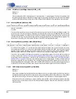
7.28
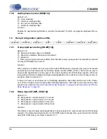
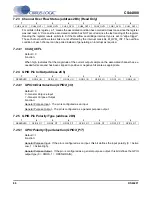
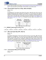
GPIO Interrupt Mask Register (address 30h)
7.28.1
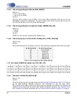
GPIO Pin Interrupt Mask (M_GPIOX)
Default = 0
Function:
General Purpose Input - The bits of this register serve as a mask for GPIO[3:0] interrupt sources. If a mask
bit is set to 1, the interrupt is unmasked, meaning that its occurrence will affect the INT pin and the Inter-
rupt Status register. If a mask bit is set to 0, the condition is masked, meaning that its occurrence will not
affect the INT pin or Interrupt Status Register. The proper pin status will be reported in the GPIO Status
Register. The bit positions align with the corresponding bits in the GPIO Status register.
General Purpose Output - This register is not used.
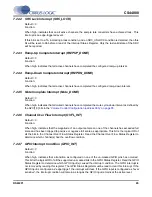
7.29
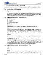
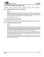
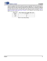
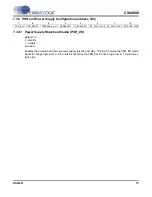
PWM Configuration Register (address 31h)
7.29.1
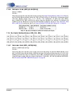
Over Sample Rate Selection (OSRATE)
Default = 0
0 - modulated PWM output pulses run at single-mode switch rate. Typically 384 kHz or 421.875 kHz.
1 - modulated PWM output pulses run at double-mode switch rate. Typically 768 kHz or 843.75 kHz.
Function:
Enables the interpolation filter in the modulator to over-sample the incoming audio to support a double-
speed PWM switch rate. This parameter can only be changed when all modulators and associated logic
are in the power-down state by setting the PDN bit in the register
“Clock Configuration and Power Control
(address 02h)” on page 51
to a 1b. Attempts to write this register while the PDN is not set will be ignored.
7.29.2
Channels A1 and B1 Output Configuration (A1/B1_OUT_CNFG)
Default = 0
0 - pwm outputs for both channels A1 and B1 are configured for half-bridge operation
1 - pwm outputs for both channels A1 and B1 are configured for full-bridge operation
Function:
Identifies the output configuration. The value selected for this bit is applicable to the outputs for channels
A1 and B1. This parameter can only be changed when all modulators and associated logic are in the pow-
er-down state by setting the PDN bit in the register
“Clock Configuration and Power Control (address 02h)”
on page 51
to a 1b. Attempts to write this register while the PDN is not set will be ignored.
7.29.3
Channels A2 and B2 Output Configuration (A2/B2_OUT_CNFG)
Default = 0
0 - pwm outputs for both channels A2 and B2 are configured for half-bridge operation
1 - pwm outputs for both channels A2 and B2 are configured for full-bridge operation
Function:
Identifies the output configuration. The value selected for this bit is applicable to the outputs for channels
A2 and B2. This parameter can only be changed when all modulators and associated logic are in the pow-
7
6
5
4
3
2
1
0
RESERVED
RESERVED
RESERVED
RESERVED
M_GPIO3
M_GPIO2
M_GPIO1
M_GPIO0
7
6
5
4
3
2
1
0
OSRATE
RESERVED
RESERVED A1/B1_OUT_CNFG A2/B2_OUT_CNFG A3_OUT_CNFG B3_OUT_CNFG A4/B4_OUT_CNFG

