DESCRIPTION AND OPERATION
FUNCTIONAL OPERATION
WBPEEUI240756A0
2 - 5
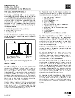
FSK INPUTS (FIELD BUS MODE) IMFEC11 ONLY
For IMFEC11 modules in the field bus mode, all data and com-
munication are FSK encoded digital signals on a shared bus
and require decoding. The microprocessor can read any input
by specifying the bus address of the device. The signal enters
the FSK communication circuitry through a transmit/receive
gate that works with the multiplexer and communication cir-
cuitry.
Figure
shows the FSK input circuit with the FSK multi-
plexer and FSK transmit/receive gate. After decoding the digi-
tal input, the FEC module can store that data in memory or
send it directly to the controlling module (MFP/MFC) through
the I/O expander bus interface.
Analog-to-Digital Converter
The FEC module can digitize analog values within the range of
-10 to +10 volts. Figure
shows the analog-to-digital conver-
sion circuitry. The analog-to-digital control chip provides the
logic needed to control the dual slope integrator. The ana-
log-to-digital conversion takes place in three stages: input inte-
gration, de-integration with a +10 or -10 volts reference and
zeroing the integrator/de-integrator.
Figure 2-3. FSK Input Circuit
TP25182A
COMMON
ACOM
15 I/O CHANNELS
INPUT
NUMBER
FSK
MULTIPLEXER
0
1
2
3
4
.
.
.
.
.
.
13
14
GATE
FSK RECEIVE
FSK TRANSMIT
TRANSMIT ENABLE
CHANNEL
SELECT
FROM
MICROPROCESSOR
TO FSK
COMMUNICATION
CIRCUITRY
0
1
2
3
.
.
11
12
13
14