DESCRIPTION AND OPERATION
FUNCTIONAL OPERATION
2 - 6
WBPEEUI240756A0
®
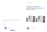
The microprocessor signals the ADC circuitry to begin convert-
ing inputs. The ADC circuitry selects the input, reference volt-
age and conversion operation through the select multiplexer.
The input signal from the select multiplexer passes through
buffers and a differential amplifier that converts the input
signal to a single ended voltage. Then the signal goes to the
input of the integrator/de-integrator stage.
The ADC circuitry selects a positive or negative reference volt-
age for this stage. Once the integrator is set to zero, the ADC
circuitry allows the integrator to run until its output reaches
the reference voltage. At this point, the ADC circuitry selects
the de-integration operation and begins a count until the zero
crossing circuit detects the signal at zero. A feedback and zero-
ing amplifier sets the integrator to zero and the process repeats
with the opposite polarity of the input and reference voltage.
The count that the ADC circuitry takes during the de-integra-
tion operation is the digital equivalent of the input. It sends
that information and the polarity to the microprocessor. The
microprocessor places it into memory and signals the ADC cir-
cuitry to begin the next conversion.
I/O Expander Bus Interface Circuitry
The FEC module uses a semicustom gate array for the I/O
expander bus interface. An integrated circuit (IC) holds all the
control logic and communication protocol. This IC circuit pro-
vides the following functions:
•
Address comparison and detection.
•
Function code latching and decoding.
•
Read strobe generation.
•
Data line filtering of bus signals.
•
On-board bus drivers.
Figure 2-4. Analog to Digital Conversion Circuitry
TP25185A
MICROPROCESSOR
REFERENCE
VOLTAGE
FILTERED
ANALOG
INPUTS
INPUT
MULTIPLEXERS
ANALOG TO
DIGITAL
CONTROL CHIP
ANALOG TO
DIGITAL
OPERATION
SELECT
MULTIPLEXER
BUFFERS AND
DIFFERENTIAL
AMPLIFIER
FEEDBACK AND
ZEROING
AMPLIFIER
DUAL SLOPE
INTEGRATOR/
DE-INTEGRATOR
ZERO-CROSSING
DETECTOR