409
8331B–AVR–03/12
Atmel AVR XMEGA AU
• TDI: Test data in. Serial input data to be shifted in to the instruction register or data register
(scan chains)
• TDO: Test data out. Serial output data from the instruction register or data register
The IEEE Std. 1149.1-2001 also specifies an optional test reset signal, TRST. This signal is not
available.
When the JTAGEN fuse is unprogrammed or the JTAG disable bit is set, the JTAG interface is
disabled. The four TAP pins are normal port pins, and the TAP controller is in reset. When
enabled, the input TAP signals are internally pulled high and JTAG is enabled for boundary scan
operations.
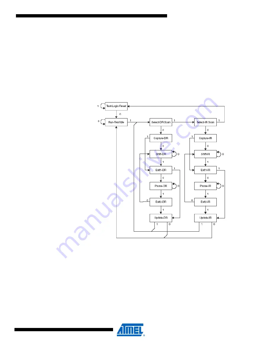
Figure 31-1.
TAP controller state diagram.
The TAP controller is a 16-state, finite state machine that controls the operation of the boundary
scan circuitry. The state transitions shown in
depend on the signal present on TMS
(shown adjacent to each state transition) at the time of the rising edge on TCK. The initial state
after a power-on reset is the test logic reset state.
Assuming the present state is run test/idle, a typical scenario for using the JTAG interface is:
• At the TMS input, apply the sequence 1, 1, 0, 0 at the rising edges of TCK to enter the shift
instruction register, or shift IR, state. While in this state, shift the four bits of the JTAG
instruction into the JTAG instruction register from the TDI input at the rising edge of TCK. The
TMS input must be held low during input of the 3 lsbs in order to remain in the shift IR state.
The msb of the instruction is shifted in when this state is left by setting TMS high. While the
instruction is shifted in from the TDI pin, the captured IR state, 0x01, is shifted out on the


