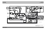
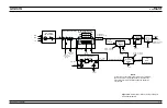
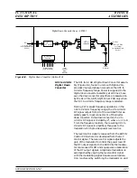


ence voltage that represents the desired RF output
power level. The resulting voltage is fed from the
A10 PCB to the ALC modulator driver circuit on the
A9 PIN Control PCB (and the ALC modulator driver
circuit on the A14 YIG, SDM, SQM Driver PCB for
>40 GHz models). The modulator control signals go
to the modulators in the switched filter assembly
and the SQM (for >40 GHz models) to adjust the RF
output power level.
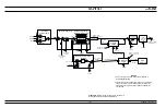
Step
Attenuators
The optional step attenuators available for use with
the 690XXB/691XXB models are as follows:
q
120 dB electronic step attenuators for
£
8.4 GHz and
£
20 GHz models (Options 2E
and 2F)
q
110 dB step attenuators for
£
20 GHz and
£
40 GHz models (Options 2A and 2B)
q
90 dB step attenuators for
£
50 GHz and
£
60 GHz models (Option 2C and 2D)
The step attenuators provide attenuation of the RF
output in 10 dB steps. The step attenuator drive
current is supplied by the A9 Control PCB.
690XXB/691XXB MM
2-31/2-32
FUNCTIONAL
RF DECK
DESCRIPTION
ASSEMBLIES
Содержание 680 C Series
Страница 4: ......
Страница 5: ......
Страница 13: ...Figure 1 1 Typical Series 690XXB 691XXB Synthesized CW Signal Generator Model 69187B Shown ...
Страница 61: ......
Страница 97: ......
Страница 205: ......
Страница 207: ......
Страница 221: ......
Страница 225: ......
Страница 241: ......
Страница 259: ......
Страница 275: ......
Страница 285: ......
Страница 289: ......
Страница 299: ......
Страница 303: ......
Страница 315: ......


