ADXL180
Rev. 0 | Page 8 of 56
V
DD
NC
V
SCO
V
CM
V
CM
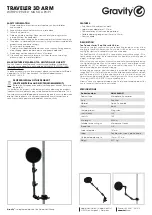
PIN CONFIGURATION AND FUNCTION DESCRIPTIONS
V
BP
V
BN
V
BC
NC
NC
NC
9
10
11
12
V
CM
NC
V
V
BN
V
CM
13
14
15
16
SCI
4
3
2
1
8
7
6
V
BN
5
V
BN
NC = NO CONNECT
DAP1
ADXL180
TOP VIEW
(Not to Scale)
DAP2
07
54
4-
0
02
Figure 3. Pin Configuration
Table 4. Pin Function Descriptions
Pin No.
Mnemonic
Description
1
NC
Reserved for Analog Devices Use Only. V
BN
or do not connect.
2 V
CM
Reserved for Analog Devices, Inc., Use Only. Do not connect.
3 V
BN
Negative
Bus
Voltage.
4
NC
Reserved for Analog Devices Use Only. V
BN
or do not connect.
5 V
DD
Voltage Regulator Bypass Capacitor.
6
NC
Reserved for ADI Use Only. V
BN
or do not connect.
7 V
SCO
Reserved for ADI Use Only. Do not connect.
8 V
BN
Negative
Bus
Voltage.
9 V
BC
Daisy-Chain Connection. Daisy-chain connection to V
BP
of the second device or do not connect.
10 V
BN
Negative
Bus
Voltage.
11 V
CM
Reserved for ADI Use Only. Do not connect.
12 V
BP
Positive
Bus
Voltage.
13
NC
Reserved for ADI Use Only. V
BN
or do not connect.
14
NC
Reserved for ADI Use Only. V
BN
or no connect
15 V
SCI
Analog Signal Chain Input. V
BN
when not in use.
16 V
CM
Reserved for ADI Use Only. Do not connect.
DAP1 V
CM
Exposed Pad: Reserved for ADI Use Only. Do not connect.
DAP2 V
BN
Exposed Pad: Negative Bus Voltage.