background image

UG-076 

Evaluation Board User Guide


Rev. A | Page 8 of 16 

PLL REFERENCE INPUT WINDOW 

The 

Reference Input Control

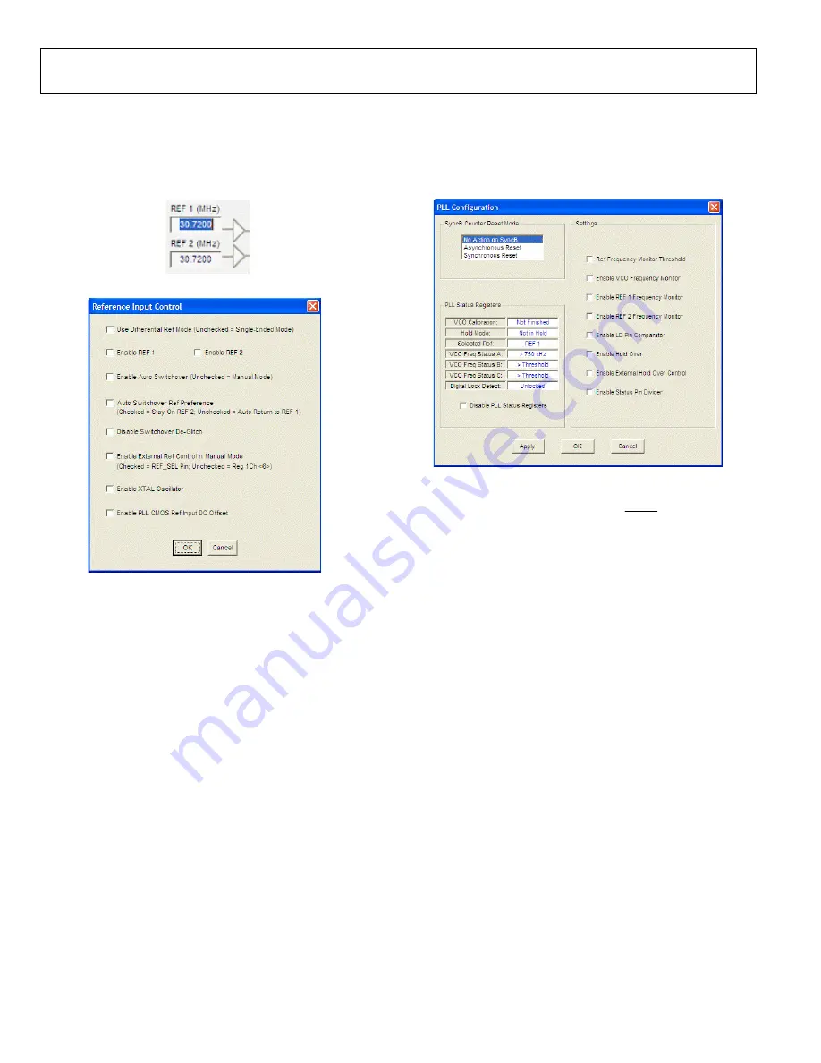
 window is shown in Figure 10 

and is accessed by clicking either of the triangular buffer 
symbols immediately to the right of the 

REF 1 (MHz)

 and 

REF 2 (MHz)

 input reference frequency boxes (see Figure 9).  

0

874

6-

024


Figure 9. Buffer Symbol 

0

87

46-

0

06


Figure 10. 

Reference Input Control

 Window 

This window is used to enable the PLL reference inputs, which 
are powered down by default. 

Select 

Enable REF 1

Enable REF 2

, or both to enable the 

appropriate reference input and click 

OK

 when finished. If a 

differential input is used, select the 

Use Differential Ref Mode 

(Unchecked = Single-Ended Mode)

 check box. Note that this 

mode must not be used simultaneously with 

Enable REF 1

 or 

Enable REF 2

.  

The remaining six check boxes control the reference switchover 
modes. If 

Disable Switchover De-Glitch

 is activated, th

AD9520


maintains the phase relationship between the active input and 
PLL output during a reference switchover. Otherwise, the 

AD9520

 minimizes the phase disturbance at the output  

during a reference switchover.  

The user must check 

Enable XTAL Oscillator

 if intending to 

connect a crystal to the reference input. 

Enable PLL CMOS Ref Input DC Offset

 forces the dc bias 

point of the single-ended reference input to be different from 
the switching point, and is useful for preventing an ac-coupled 
input from chattering when the reference input is lost. 

PLL CONFIGURATION WINDOW 

The 

PLL Configuration

 window shown in Figure 11 is opened 

by clicking the 

Config PLL

 button on the main screen. The 

window has three sections: 

SyncB Counter Reset Mode

PLL 

Status Registers

, and 

Settings

087

46

-00

7


Figure 11. 

PLL Configuration

 Window 

The 

SyncB Counter Reset Mode

 section indicates whether the 

R, A, and B counters are reset when the SYNC pin is activated, 
and controls Register 0x019, Bits[7:6]. See th

AD9520

 data 

sheet for more details. 

The 

PLL Status Registers

 section allows the user to see the 

current value of the readonly PLL status register, Address 0x01F. 
This function is useful for ensuring that th

AD9520

 VCO has 

finished VCO calibration, and that the PLL is locked. 

The 

Settings

 section controls the various PLL settings such  

as holdover. The 

AD9520

 data sheet describes these functions 

in detail. 

REFMON, STATUS, AND LD BUTTONS 

These three blue buttons (

REFMON

STATUS

, and 

LD

) allow 

the user to select which signals appear at the REFMON, 
STATUS, and LD pins at Connector P1. Connector P1 is located 
in the center of the evaluation board. The pins in the left 
column of Connector P1 are ground pins, and the ones in the 
right column are signal pins.


There are many useful diagnostic signals available at these  
pins. The R divider output is particularly useful. In the example 
used in the Quick Start Guide to the AD9520 PLL section, the 
80 kHz signal is visible on the STATUS pin to ensure that the 
reference inputs and R divider are working properly. 

Dynamic signals (such as the R divider output) are primarily 
intended for diagnostics. These diagnostic signals may adversely 
affect PLL performance in critical applications if left on in 
normal operation.  

Содержание AD9520-0

Страница 1: ...are very low noise phase locked loop PLL clock synthesizers featuring an integrated voltage controlled oscillator VCO clock dividers and up to 24 outputs The AD9520 product series features automatic...

Страница 2: ...D9520 on a User Board 15 AD9520 Binary File Generation 16 Checksum Generation 16 Avoiding Checksum Mismatches 16 REVISION HISTORY 5 2017 Rev 0 to Rev A Changes to Title and General Description Section...

Страница 3: ...ng is recommended in applications requiring automatic hitless reference switching There is a possibility that the AD9520 receive buffer can chatter when an ac coupled clock stops toggling Connect an o...

Страница 4: ...ing that the evaluation board was found or red text appears indicating that the evaluation board was not found 2 If the evaluation board is found click anywhere in the pop up window with the Evaluatio...

Страница 5: ...p from the PLL MODE box found at the top of the main window see Figure 8 2 Enter the intended reference input frequency in megahertz in the REF 1 MHz box at the upper left corner of the main window 3...

Страница 6: ...f the CHARGE PUMP box However this setting normally does not need to be modified 11 Set the VCO divider by clicking the green VCO box in the center of the main window immediately to the left of the Ca...

Страница 7: ...are listed in the following sections and each of these subsections has its own window From the main window each functional block can be accessed by clicking that block in the main window When a subwi...

Страница 8: ...N WINDOW The PLL Configuration window shown in Figure 11 is opened by clicking the Config PLL button on the main screen The window has three sections SyncB Counter Reset Mode PLL Status Registers and...

Страница 9: ...ssed by clicking the EEPROM button near the lower left corner of the main window 08746 008 Figure 12 EEPROM Control Window To store the current register settings of the AD9520 to the EEPROM click the...

Страница 10: ...der value For example it is not possible to use the internal VCO and a feedback divider of 30 However the R divider can be doubled which allows a feedback divider of 60 The feedback divider window has...

Страница 11: ...king the Cal VCO button in the main window 08746 015 Figure 19 Calibrate VCO Window A valid reference input signal must be present to complete VCO calibration and the VCO must be recalibrated any time...

Страница 12: ...istors on each output This termination scheme is ideal for LVPECL drivers However this scheme degrades the CMOS driver performance Improved CMOS driver performance is achieved by removing the 200 pull...

Страница 13: ...ted evaluation board see Figure 25 08746 019 Figure 25 Select USB Device Window Configure Serial Port The I O Interface window allows the user to control how the USB controller interacts with the AD95...

Страница 14: ...better choice Typical phase detector frequencies for these applications are 10 MHz to 100 MHz and typical loop bandwidths for this loop filter are 50 kHz to 500 kHz depending on the configuration The...

Страница 15: ...and then click Detect Current Configuration A dialog box appears and acknowledges the I2 C mode and address The evaluation software starts at I2 C Address 0x058 and stops at the first valid I2 C addre...

Страница 16: ...MA 02062 USA Subject to the terms and conditions of the Agreement ADI hereby grants to Customer a free limited personal temporary non exclusive non sublicensable non transferable license to use the Ev...

Отзывы: